
User manual

Memory Controller
MPC8260 PowerQUICC II Family Reference Manual, Rev. 2
Freescale Semiconductor 11-71
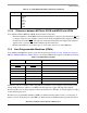
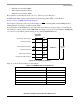
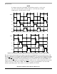
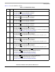
Table 11-36 describes RAM word fields.
Table 11-36. RAM Word Bit Settings
Bit Name Description
0 CST1 Chip-select timing 1. Defines the state of CS
during clock phase 1.
0 The value of the CS
line at the rising edge of T1 will be 0
1 The value of the CS
line at the rising edge of T1 will be 1
See Section 11.6.4.1.1, “Chip-Select Signals (CxTx).”
1 CST2 Chip-select timing 2. Defines the state of CS
during clock phase 2.
0 The value of the CS
line at the rising edge of T2 will be 0
1 The value of the CS
line at the rising edge of T2 will be 1
2 CST3 Chip-select timing 3. Defines the state of CS
during clock phase 3.
0 The value of the CS
line at the rising edge of T3 will be 0
1 The value of the CS
line at the rising edge of T3 will be 1
3 CST4 Chip-select timing4. Defines the state of CS
during clock phase 4.
0 The value of the CS
line at the rising edge of T4 will be 0
1 The value of the CS
line at the rising edge of T4 will be 1
4 BST1 Byte-select timing 1. Defines the state of BS
during clock phase 1.
0 The value of the BS
lines at the rising edge of T2 will be 0
1 The value of the BS
lines at the rising edge of T2 will be 1
The final value of the BS
lines depends on the values of BRx[PS], the TSIZ lines, and A[30–31] for
the access. See Section 11.6.4.1.2, “Byte-Select Signals (BxTx).”
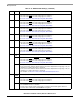
5 BST2 Byte-select timing 2. Defines the state of BS
during clock phase 2.
0 The value of the BS
lines at the rising edge of T2 will be 0
1 The value of the BS
lines at the rising edge of T2 will be 1
The final value of the BS
lines depends on the values of BRx[PS], TSIZ
x
, and A[30–31] for the
access.
6 BST3 Byte-select timing 3. Defines the state of BS
during clock phase 3.
0 The value of the BS
lines at the rising edge of T3 will be 0
1 The value of the BS
lines at the rising edge of T3 will be 1
The final value of the BS
lines depends on the values of BR
x
[PS], TSIZ
x
, and A[30–31] for the
access.
7 BST4 Byte-select timing 4. Defines the state of BS
during clock phase 4.
0 The value of the BS
lines at the rising edge of T4 will be 0
1 The value of the BS
lines at the rising edge of T4 will be 1
The final value of the BS
lines depends on the values of BRx[PS], TSIZ
x
, and A[30–31] for the
access.
8–9 G0L General-purpose line 0 lower. Defines the state of GPL0
during phases 1–2.
00 The value of GPL0
at the rising edge of T1 is as defined in M
x
MR[G0CL]
10 The value of the GPL0
line at the rising edge of T1 will be 0
11 The value of the GPL0
line at the rising edge of T1 will be 1
See Section 11.6.4.1.3, “General-Purpose Signals (GxTx, GOx).”
10–11 G0H General-purpose line 0 higher. Defines the state of GPL0
during phase 3–4.
00 The value of GPL0
at the rising edge of T3 is as defined in M
x
MR[G0CL]
10 The value of the GPL0
line at the rising edge of T3 will be 0
11 The value of the GPL0
line at the rising edge of T3 will be 1
See Section 11.6.4.1.3, “General-Purpose Signals (GxTx, GOx).”