
User manual

Memory Controller
MPC8260 PowerQUICC II Family Reference Manual, Rev. 2
Freescale Semiconductor 11-81
to logic 0) at the end of that cycle, unless there is a back-to-back UPM cycle pending. In many cases
this allows the UPM routine to finish one cycle earlier because it is now possible and desired to
assert both UTA and LAST.
• MCR is eliminated—In the PowerQUICC II, MCR is eliminated. The function of RAM read/write
and RUN is done via the MxMR.
• UTA polarity is reversed—In the PowerQUICC II, UTA is active-high.
• The disable timer control (TODT) and LAST bit in the RAM array word must be set together,
otherwise TODT is ignored.
• Refresh timer value is in a separate register—In the PowerQUICC II, the refresh timer value has
moved to two registers, PURT and LURT, which can serve multiple UPMs.
• Refresh on the 60x bus must be done in UPMA; on the local bus, it must be done in UPMB.
• New feature: Repeated execution of the current RAM word (REDO).
• Extended hold time on reads can be up to 8 clock cycles instead of 1 in the MPC8xx.
• Each UPM on the MPC8xx has a wait signal. On the PowerQUICC II, the three UPMs share two
wait signals (PUPMWAIT and LUPMWAIT).
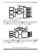
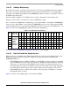
11.7 Memory System Interface Example Using UPM
Connecting the PowerQUICC II to a DRAM device requires a detailed examination of the timing diagrams
representing the possible memory cycles that must be performed when accessing this device. This section
provides timing diagrams for various UPM configurations.
Figure 11-67. DRAM Interface Connection to the 60x Bus (64-Bit Port Size)
RAS
CAS[0–1]
W
1M x 16
16
A[0–9]
D[0–15]
RAS
CAS[0–1]
W
1M x 16
16
A[0–9]
D[0–15]
PowerQUICC II
BS[0–7]
CS1
BCTL0
A[19–28]
D[0–63]
RAS
CAS[0–1]
W
1M x 16
16
A[0–9]
D[0–15]
RAS
CAS[0–1]
W
1M x 16
16
A[0–9]
D[0–15