
User manual


Memory Controller
MPC8260 PowerQUICC II Family Reference Manual, Rev. 2
11-92 Freescale Semiconductor
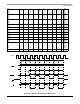
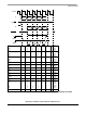
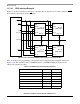
11.7.0.1 EDO Interface Example
Figure 11-76 shows a memory connection to extended data-out type devices. For this connection, GPL1
is connected to the memory device’s OE pins.
Figure 11-76. PowerQUICC II/EDO Interface Connection to the 60x Bus
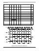
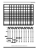
Table 11-44 shows the programming of the register field for supporting the configuration shown in
Figure 11-76. The example assumes a CLKIN frequency of 66 MHz and that the device needs a
1,024-cycle refresh every 10 µs.
Table 11-44. EDO Connection Field Value Example
Explanation Field Value
Machine select UPMA BR
x
[MS] 0b100
Port size 64-bit BR
x
[PS] 0b00
No write protect (R/W) BR
x
[WP] 0b0
Refresh timer prescaler MPTPR 0x04
Refresh timer value (1024 refresh cycles) PURT[PURT] 0x07
Refresh timer enable M
x
MR[RFEN] 0b1
Address multiplex size M
x
MR[AM
x
] 0b001
RAS
CASl/h
W
MCM516165
1M x 16
16
A[0–9]
D[0–15]
16
PowerQUICC II
BS[0–7]
CS1
R/W
A[19–28]
D[0–63]
16
16
OE
RAS
CASl/h
W
MCM516165
1M x 16
A[0–9]
D[0–15]
OE
RAS
CASl/h
W
MCM516165
1M x 16
A[0–9]
D[0–15]
OE
RAS
CASl/h
W
MCM516165
1M x 16
A[0–9]
D[0–15]
OEGPL1