
User manual

Communications Processor Module Overview
MPC8260 PowerQUICC II Family Reference Manual, Rev. 2
Freescale Semiconductor 14-3
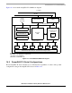
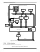
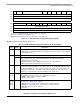
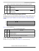
Figure 14-1 shows the PowerQUICC II’s CPM block diagram.
Figure 14-1. PowerQUICC II CPM Block Diagram
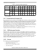
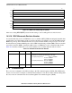
14.2 PowerQUICC II Serial Configurations
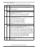
The PowerQUICC II offers a flexible set of communications capabilities. A subset of the possible
configurations using an PowerQUICC II is shown in Table 14-1.
Baud Rate Generators
60x Bus
2 MCCs
1
3 FCCs
2
4 SCCs 2 SMCs SPI I
2
C
To S I U
4 Timers
Parallel I/O Ports
Bus Interface SDMA
Dual-Port
RAM
Communications
ROM
Internal Bus
Peripheral Bus
Serial Interface (SI), TC layer
3
, and Time-Slot Assigner (TSA)
Interrupt
Controller
Local Bus
Processor
Note
1
One MCC on the MPC8250 and MPC8255
2
Two FCCs on the MPC8255
3
MPC8264 and MPC8266 only