
User manual

Serial Interface with Time-Slot Assigner
MPC8260 PowerQUICC II Family Reference Manual, Rev. 2
Freescale Semiconductor 15-29
device negates L1GRx. The PowerQUICC II then stops sending and retransmits the frame when L1GRx
is reasserted. This procedure is handled automatically for the first two buffers of a frame.
For the primary rate IDL, the PowerQUICC II supports up to four 8-bit channels in the frame, determined
by the SIx RAM programming. To support more channels, the user can route more than one channel to
each SCC and the SCC treats it as one high-speed stream and store it in the same data buffers (appropriate
only for transparent data). Additionally, the PowerQUICC II can be used to assert strobes for support of
additional external IDL channels.
The IDL interface supports the CCITT I.460 recommendation for data-rate adaptation since it separately
accesses each bit of the IDL bus. The current-route RAM specifies which bits are supported by the IDL
interface and by which serial controller. The receiver only receives bits that are enabled by the receiver
route RAM. Otherwise, the transmitter sends only bits that are enabled by the transmitter route RAM and
three-states L1TXDx.
15.6.2 IDL Interface Programming
To program an IDL interface, first program SIxMR[GMx] to the IDL grant mode for that channel. If the
receive and transmit sections interface to the same IDL bus, set SIxMR[CRTx] to internally connect the
Rx clock and sync signals to the transmit section. Then, program the SIx RAM used for the IDL channels
to the preferred routing. See Section 15.4.4, “SIx RAM Programming Example.”
Define the IDL frame structure by programming SIxMR[xFSDx] to have a 1-bit delay from frame sync to
data, SIxMR[FEx] to sample on the falling edge, and SIxMR[CEx] to transmit on the rising edge of the
clock. Program the parallel I/O open-drain register so that L1TXDx is three-stated when inactive; see
Section 40.2.1, “Port Open-Drain Registers (PODRA–PODRD).” To support the D channel, program the
appropriate CMXSCR[GRx] bit, as described in Section 16.4.5, “CMX SCC Clock Route Register
(CMXSCR),” and program the SIx RAM entry to route data to the chosen serial controller. The two
definitions of IDL, 8 or 10 bits, are implemented by simply modifying the SIx RAM programming. In both
cases, L1GRx is sampled while L1TSYNCx is asserted and transferred to the D-channel SCC as a grant
indication.
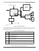
For example, based on the same 10-bit format as in Section 15.4.4, “SIx RAM Programming Example,”
implement an IDL bus using SCC1, SCC2, and SMC1 connected to TDMa1 as follows:
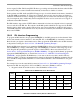
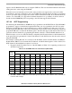
1. Program both the Tx and Rx sections of the SIx RAM as in Table 15-10.
Table 15-10. SI
x
RAM Entries for an IDL Interface
Entry
Number
SI
x
RAM Entry
MCC SWTR SSEL CSEL CNT BYT LST Description
0 0 0 0000 0010 000 1 0 8-bit SCC2
1 0 0 0000 0001 000 0 0 1-bit SCC1
2 0 0 0000 0000 000 0 0 1-bit no
support
3 0 0 0000 0101 011 0 0 4-bit SMC1