
User manual
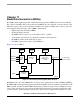

Timers
MPC8260 PowerQUICC II Family Reference Manual, Rev. 2
18-4 Freescale Semiconductor
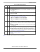
Table 18-1 describes TGCR1 fields.
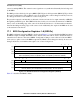
The TGCR2 register is shown in Figure 18-4.
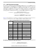
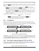
01234567
Field CAS2 — STP2 RST2 GM1 — STP1 RST1
Reset 0000_0000
R/W R/W
Addr 0x0x10D80
Figure 18-3. Timer Global Configuration Register 1 (TGCR1)
Table 18-1. TGCR1 Field Descriptions
Bits Name Description
0 CAS2 Cascade timers.
0 Normal operation.
1 Timers 1 and 2 cascade to form a 32-bit timer.
1 — Reserved, should be cleared.
2 STP 2 Stop timer.
0 Normal operation.
1 Reduce power consumption of the timer. This bit stops all clocks to the timer, except the clock
from the internal bus interface, which allows the user to read and write timer registers. The clocks
to the timer remain stopped until the user clears this bit or a hardware reset occurs.
3 RST2 Reset timer.
0 Reset the corresponding timer (a software reset is identical to an external reset).
1 Enable the corresponding timer if the STP bit is cleared.
4 GM1 Gate mode for TGATE1
. This bit is valid only if the gate function is enabled in TMR1 or TMR2.
0 Restart gate mode. TGATE1
is used to enable/disable count. A falling TGATE1 enables and
restarts the count and a rising edge of TGATE1
disables the count.
1 Normal gate mode. This mode is the same as 0, except the falling edge of TGATE1
does not
restart the count value in TCN.
5 — Reserved, should be cleared.
6 STP1 Stop timer.
0 Normal operation.
1 Reduce power consumption of the timer. This bit stops all clocks to the timer, except the clock
from the internal bus interface, which allows the user to read and write timer registers. The clocks
to the timer remain stopped until the user clears this bit or a hardware reset occurs.
7 RST1 Reset timer.
0 Reset the corresponding timer (a software reset is identical to an external reset).
1 Enable the corresponding timer if STP = 0.