
User manual
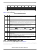

Timers
MPC8260 PowerQUICC II Family Reference Manual, Rev. 2
Freescale Semiconductor 18-7
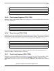
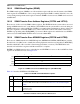
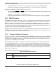
18.2.5 Timer Capture Registers (TCR1–TCR4)
Each timer capture register (TCR1–TCR4), shown in Figure 18-7, is used to latch the value of the counter
according to TMRx[CE].
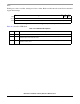
18.2.6 Timer Counters (TCN1–TCN4)
Each timer counter register (TCN1–TCN4), shown in Figure 18-8, is an up-counter. A read cycle to TCNx
yields the current value of the timer but does not affect the counting operation. A write cycle to TCNx sets
the register to the written value, thus causing its corresponding prescaler, TMRx[PS], to be reset.
Note that the counter registers may not be updated correctly if a write is made while the timer is not
running. Use TRRx to define the preferred count value.
18.2.7 Timer Event Registers (TER1–TER4)
Each timer event register (TERx), shown in Figure 18-9, reports events recognized by the timers. When
an output reference event is recognized, the timer sets TERx[REF] regardless of the corresponding
TMRx[ORI]. The capture event is set only if it is enabled by TMRx[CE]. TER1–TER4 can be read at any
time.
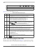
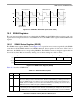
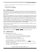
0 15
Field Timeout reference value
Reset 0xFFFF
R/W R/W
Addr 0x0x10D94 (TRR1), 0x0x10D96 (TRR2), 0x0x10DA4 (TRR3), 0x0x10DA6 (TRR4)
Figure 18-6. Timer Reference Registers (TRR1–TRR4)
0 15
Field Latched counter value
Reset 0x0000
R/W R/W
Addr 0x0x10D98 (TCR1), 0x0x10D9A (TCR2), 0x0x10DA8 (TCR3), 0x0x10DAA (TCR4)
Figure 18-7. Timer Capture Registers (TCR1–TCR4)
0 15
Field Up counter
Reset 0x0000
R/W R/W
Addr 0x0x10D9C (TCN1), 0x0x10D9E (TCN2), 0x0x10DAC (TCN3), 0x0x10DAE (TCN4)
Figure 18-8. Timer Counter Registers (TCN1–TCN4)