
User manual
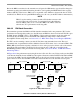

ATM Controller and AAL0, AAL1, and AAL5
MPC8260 PowerQUICC II Family Reference Manual, Rev. 2
Freescale Semiconductor 30-39
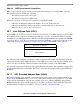
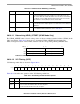
30.10.1.1 Determining UEAD_OFFSET (UEAD Mode Only)
The UEAD_OFFSET value is based on the position of the user-defined extended address (UEAD) in the
UDC extra header. Table 30-12 shows how to determine UEAD_OFFSET: first determine the
halfword-aligned location of the UEAD, and then read the corresponding UEAD_OFFSET value.
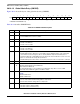
30.10.1.2 VCI Filtering (VCIF)
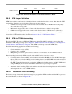
VCI filtering enable bits are shown in Figure 30-22.
Table 30-13 describes the operation of the VCI filtering enable bits.
0xB0 TCR Hword (ABR only) Tag cell rate. The minimum cell rate allowed for all ABR
channels. An ABR channel whose ACR is less than TCR sends only
out-of-rate F-RM cells at TCR. Should be set to 10 cells/sec as defined in
the TM 4.0. Uses the ATMF TM 4.0 floating-point format. Note that the
APC minimum cell rate (MCR) should be at least TCR.
0xB2 ABR_RX_TCTE Hword (ABR only) Points to total of 16 bytes reserved dual-port RAM area used
by the CP. Should be 16-byte aligned. User-defined offset from dual-port
RAM base.
— Additional parameters — • For additional AAL1 CES parameters, refer to Table 31-4.
• For additional AAL2 parameters, refer to Table 32-13.
1
Offset from FCC base: 0x8400 (FCC1) and 0x8500 (FCC2); see Section 14.5.2, “Parameter RAM.”
Offset
0151631
0x0 UEAD_OFFSET = 0x2 UEAD_OFFSET = 0x0
0x4 UEAD_OFFSET = 0x6 UEAD_OFFSET = 0x4
0x8 UEAD_OFFSET = 0xA UEAD_OFFSET = 0x8
Table 30-12. UEAD_OFFSETs for Extended Addresses in the UDC Extra Header
012 3 4 5678910 1112131415
Field 0 0 0 VC3 VC4 0 VC6 VC7 VC8 VC9 VC10 VC11 VC12 VC13 VC14 VC15
Figure 30-22. VCI Filtering Enable Bits
Table 30-13. VCI Filtering Enable Field Descriptions
Bits Name Description
0–2, 5 — Clear these bits.
3, 4, 6,
7–15
VC
x
VCI filtering enable
0 Do not send cells with this VCI to the raw cell queue.
1 Send cells with this VCI to the raw cell queue.
Table 30-11. ATM Parameter RAM Map (continued)
Offset
1
Name Width Description