M9328MX21ADSE Application Development System User’s Manual Document Number: UMS-21100 Rev.
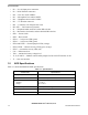
Chapter 1 General Information 1.1 1.2 1.3 1.4 1.5 Description . . . . . . . . . . . . . . . . . . . . . . . . . . . . . . . . . . . . . . . . . . . . . . . . . . . . . . . . . . . . . . . . . M9328MX21ADSE Features . . . . . . . . . . . . . . . . . . . . . . . . . . . . . . . . . . . . . . . . . . . . . . . . . . . System and User Requirements . . . . . . . . . . . . . . . . . . . . . . . . . . . . . . . . . . . . . . . . . . . . . . . . . M9328MX21ADSE Diagram . . . . . . . . . . . . . . . . . . . . . . .
3.5 3.6 3.7 3.8 3.9 3.10 3.11 3.12 3.13 3.14 Multi-ICE Connector . . . . . . . . . . . . . . . . . . . . . . . . . . . . . . . . . . . . . . . . . . . . . . . . . . . . . . . . Ethernet Connector . . . . . . . . . . . . . . . . . . . . . . . . . . . . . . . . . . . . . . . . . . . . . . . . . . . . . . . . . . USB OTG Connector . . . . . . . . . . . . . . . . . . . . . . . . . . . . . . . . . . . . . . . . . . . . . . . . . . . . . . . . NAND Flash Connector . . . . . . . . . . . . . . . . . . . . . . . .
About This Book This manual explains how to connect and operate the M9328MX21ADS i.MX21 Application Development System. Audience The audience for this manual is handheld communication device designers. It is assumed that users are engineers or technicians with experience using development systems. Organization The manual consists of three chapters. • Chapter 1 General Information introduces the user to the features and capabilities of the ADS.
Definitions, Acronyms, and Abbreviations The following acronyms and abbreviations are used in this manual. This list does not include signal, register, and software mnemonics.
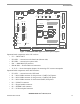
Chapter 1 General Information 1.1 Description The M9328MX21ADSE helps you develop applications for the i.MX21 MCU. The ADS has 19 connectors and sockets that support application software, target board debugging, and optional circuit cards. A separate LCD display panel and a separate keypad are supplied with the ADS. When you connect the LCD panel and keypad to the ADS Base board, they align with each other. 1.2 M9328MX21ADSE Features ADS features include: • i.
General Information • • • • • • • • • • • 1.3 Separate CMOS Image Sensor Card Audio CODEC includes an 11.28 MHz crystal oscillator, a 3.5 mm audio input jack, a 3.5 mm microphone jack, and a 3.5 mm headphone jack Cirrus Logic CS8900A-CQ3Z Ethernet controller, with RJ-45 connector for connecting to a system hub Two 32 × 3-pin DIN expansion connectors with most i.
General Information OFF P8 P3 ON P2 EXT UART DCE SW1 SD2_D1 SD2_D0 J3 BASE BOARD NC NC SD2_D2 SD2_D3 J5 J4 P7 IrDA USB OTG RI CD DSR NC ACT U16 UART1 DCE DTR P9 ETHERNET F1 2A P4 P1 UART4 DTE 3 2 1 VR1 BATT EM J6 LCD CON +5V IN CPU BOARD PX1/PY1 LINK ACT P20 MULTI-ICE S2 BOOT0 BOOT1 BOOT2 BOOT3 CLKMODE0 CLKMODE1 SW1 IRQ SW2 READ 1 2 3 4 5 6 7 8 LED1 LED2 LED3 LED4 LED7 BUZZER NAND FLASH CARD 5V PWR VCC PWR STAT2 STAT1 BUS ACT PK1 S1 1 2 3 4 5 6 7 8 P10 LINE IN
General Information • • • • • • • • • • • • • • • • • • • • • 1.5 P8 — 5.
Configuration and Operation Chapter 2 Configuration and Operation 2.1 Introduction This section contains configuration information, connection descriptions, and other operational information that may be useful during the development process. 2.2 Configuring Board Components Table 2-1 is a summary of configuration settings. The following paragraphs provide additional information about configuring and using the ADS. Table 2-1.
Configuration and Operation Table 2-1. Component Configuration Settings (continued) Component Position Modem Control Enable Jumpers (on Base board) J3, DTR J4, DSR J5, CD J6, RI 2.2.1 1 2 3 1 2 3 Effect The specified RS-232 control signal of P2 connects to the specified I/O signal.
Configuration and Operation ON 1 2 3 4 5 6 7 8 UART1_ON UART4_ON IrDA_ON NEXUS_ON, (Set to OFF) JTAG_CTRL, (Set to OFF) TONE_OUT PEN_CS_B PEN_IRQ_B S1 Figure 2-1. Switch S1 2.2.2 Mode/User Switch (S2) S2 is a DIP switch that consists of eight slide switches. S2-1 to S2-4 configure boot mode and S2-5 and S2-6 control the clock bypass modes. These switch settings take effect only on power up or after a reset. S2 also provides two user definable switches (S2-7 and S2-8).
Configuration and Operation 2.3 Operation This section describes how the system functions and how to use the boards. 2.3.1 Functional Block Diagram Figure 2-3 shows the functional interconnections of the ADS in a block diagram format.
Configuration and Operation VCC VCC VCC 8MX16-Bit Burst Flash CS0 CS WP ACC 8MX16-Bit Burst Flash ECB RDY A2...A24 A0...A22 BCLK OE LBA DQM3_EB3 FLASH_RST CLK OE AVD WE RESET D0.15 D0..15 DQM1_EB1 WE D16..31 D0.15 Figure 2-4. Burst Flash Interface VCC 16MX16-Bit SDRAM CS2 SDCKE0 SDCLK RAS CAS WE CS CKE CLK RAS CAS WE A2..A18 A0..10 BA0 A19 A20 DQM1_EB1 DQM0_EB0 A11 BA0 BA1 LDQM UDQM D0..15 D0..15 16MX16-Bit SDRAM DQM3_EB3 DQM2_EB2 LDQM UDQM D16..31 D0..15 Figure 2-5.
Configuration and Operation the entire 64 MB address space allowed for CSD0, but the Burst Flash occupies only 32 MB of the 64 MB space available to CS0, so it appears in two different ranges of addresses. CS1 covers 16 MB allowing many repetitions of the memory mapped peripherals. Table 2-4.
Configuration and Operation i.MX21 RS232 Transceiver VCC P1 UART1_TXD1 UART1_RXD1 UART1 UART1_RTS1 DCE EN UART1_CTS1 S1-1 GND Software Enable via MMIO Latch RS232 Transceiver USBH1_TXDM USBH1_RXDP USBH1_RXDM USBH1_RXDP TXD4 RXD4 RTS CTS SD2_D1 DSR* SD2_D2 CD* SD2_D3 RI* SD2_D0 DTR* P2 UART4 VCC DTE EN S1-2 * If enabled by jumper GND Buffer Software Enable via MMIO Latch IrDA UART3_TXD UART3_RXD VCC EN EN S1-3 GND Software Enable via MMIO Latch Figure 2-7.
Configuration and Operation i.MX21 VCC CS8900A-CQ3Z SA8 SA9 Isolation Transformer SA0 SA4..7 SA10..19 BA1..3 SA1..3 D0..15 D0..15 P9 RJ45 Connector AEN CS_LAN B_OE IOR IOW B_RW B_DQM3_EB3 UART3_RTS SBHE INTRQ0 CHIPSEL Figure 2-8. Ethernet Interface 2.3.7 Touchscreen ADC The ADS is equipped with an Analog Devices AD7873BRQZ ADC. The ADC communicates with the touchscreen of the LCD on the Base board.
Configuration and Operation 2.3.8 CD Quality CODEC The ADS has a Wolfson WM8731SEDS 32-bit linear low power stereo CODEC with a built-in headphone driver (U24). The CODEC is controlled by the i.MX21, which sends the digital audio data via an SSI2 interface and control data via an I2C interface. The CODEC has stereo line and mono microphone level audio inputs as well as stereo headphone outputs.
Configuration and Operation 2.3.10 Memory Mapped I/O The ADS uses Memory Mapped I/O to add I/O functions without using the I/O resources of the processor. The following paragraphs describe the I/O functions. 2.3.10.1 Input I/O A memory read of hex address 0xCC80_0000 inputs the state of the ADS signals connected to latches U5 and U7. Table 2-7 shows which signal is associated with each data bit. Table 2-7.
Configuration and Operation 2.3.10.2 Output I/O A memory write to hex address 0xCC80_0000 causes U5 and U7 to latch the logic state of the data bus. Each latch output is associated with the data bus signal of the same number (Bit 0 is equal to DATA0, and so on). All output bits are forced to logic 0 (low) on power up or reset. Table 2-8 shows the functions associated with each data bit. Table 2-8.
Configuration and Operation 2.3.11 Audio Indicator (Buzzer) The ADS includes an audio indicator or buzzer, U23. When S1-6 is ON, the PWMO pin of the i.MX21 controls this function. This buzzer operates from 1 KHz to 10 KHz. The maximum sound level is reached when the frequency is 3 KHz and the duty cycle is 50%. 2.3.12 LED Indicators Table 2-9 shows the ADS LED indicators and their associated functions. Table 2-9.
Configuration and Operation Table 2-10. M9328MX21ADSE Connectors (continued) Connector 2.5 Function Comments P9 Ethernet Standard Ethernet connector. A cable for direct network and one for crossover connections (direct to a PC) have been provided. P10 Line In Standard 3.5 mm connector for stereo audio input to the WM8731SEDS CODEC P11 Microphone In Standard 3.5 mm connector for a microphone. Use only dynamic microphones with a 200 to 600 ohms impedance. P12 Headphone Standard 3.
Configuration and Operation OFF P8 P3 ON P2 EXT UART DCE SW1 U16 UART1 DCE DTR P9 ETHERNET F1 2A P4 P1 UART4 DTE ACT NC NC NC SD2_D0 SD2_D1 SD2_D2 SD2_D3 J3 BASE BOARD J4 3 2 1 VR1 BATT EM J6 J5 TFT LCD PANEL (240 x 320 dots) CPU BOARD PX1/PY1 34 CONDUCTOR RIBBON CABLE ACT MULTI-ICE P20 PK1 LED1 LED2 LED3 LED4 LED7 BUZZER P10 LINE IN BOOT0 BOOT1 BOOT2 BOOT3 CLKMODE0 CLKMODE1 SW1 IRQ SW2 READ 1 2 3 4 5 6 7 8 S1 1 2 3 4 5 6 7 8 NAND FLASH CARD S2 5V PWR VCC PWR STAT2
Configuration and Operation P1 EXT UART DCE SW1 P9 ETHERNET F1 2A UART4 DTE U16 UART1 DCE DTR SD2_D1 J3 NC NC SD2_D2 SD2_D3 J4 J2 P7 IrDA USB OTG RI CD DSR NC ACT SD2_D0 BASE BOARD P4 P1 J5 3 2 1 VR1 BATT EM J6 CPU BOARD PX1/PY1 P2 P20 MULTI-ICE BUZZER PK1 BOOT0 BOOT1 BOOT2 BOOT3 CLKMODE0 CLKMODE1 SW1 IRQ SW2 READ 1 2 3 4 5 6 7 8 LED1 LED2 LED3 LED4 LED7 S1 1 2 3 4 5 6 7 8 P10 LINE IN UART1_ON UART4_ON IrDA_ON NEXUS_EN JTAG_CTRL TONE_OUT PEN_CS_B PEN_IRQ_B NAND FLASH C
Configuration and Operation 2.5.2 Using the Keypad To use the keypad module, connect the 20 conductor ribbon cable supplied with the ADS from connector P1 of the Keypad module to P5 of the M9328MX21ADSE Base board. 2.5.3 Using a NAND Flash Card CAUTION To avoid circuit damage, do not plug-in the NAND Flash card with power applied to the board. To use the NAND Flash module supplied with the ADS, connect PN1 & PN2 of the NAND Flash module to PM1 & PM2 on the CPU board.
Configuration and Operation 2.5.7 Using the TV Encoder Card A TV encoder card is supplied with the ADS. The main component is a FS453LF (PC to TV Video Scan converter) from FOCUS Enhancements Semiconductor. For details on TV encoder operation, refer to its data sheet, available at http://www.focusinfo.com/ CAUTION Make sure that input power is disconnected or switched off before the TV encoder card is installed. Connecting the card with power applied can damage the TV encoder card and the Base board.
Configuration and Operation M9328MX21ADSE User’s Manual, Rev.
Chapter 3 Support Information 3.1 Introduction This section contains connector pin assignments, connector signal descriptions, and other useful information about the M9328MX21ADSE. Both the CPU and Base board connectors are described. The tables in this section list signal names as they appear in the schematics for the boards. The figures usually refer to the same signal name, but may substitute a generally accepted standard name for that function.
Support Information PX1 OE_ACD FLM_VSYNC_SPS SPL_SPR VCC CLS LSCLK LD16_R4 LD14_R2 LD12_R0 LD10_G4 LD8_G2 LD6_G0 LD4_B4 LD2_B2 LD0_B0 UART3_RXD UART3_TXD USBG_RXDP USBG_RXDM USBG_TXDP USBG_TXDM USBG_SDA P5V USBH1_TXDP USBH1_TXDM USBH1_RXDP USBH1_RXDM USB_BYP_B P5V TP22 CLK_26 UART1_RTS UART1_RXD UART2_RTS UART2_RXD BOOT3 BOOT1 PWM0 JTAG_CTRL RESET_IN_B POR_B CLKMODE0 B_CS5_B B_CS1_B B_OE_B B_NEXUSEVTI B_A0 B_A2 B_D7 B_D6 B_D5 B_D4 B_D3 B_D2 B_D1 B_D0 B_A20 B_A22 B_A24 TP25 1 3 5 7 9 11 13 15 17 19 21 23 2
Support Information Table 3-1. CPU to Base Board PX1/PY1 Connector Signals Pin(s) Signal 1 OE_ACD 2, 7, 30, 62 VCC 3 Description OUTPUT ENABLE / ALTERNATE CRYSTAL DIRECTION +3.0 VDC power FLM_VSYNC_SPS FIRST LINE MARKER / VERTICAL SYNCHRONIZATION 4 CONTRAST LCD bias voltage used as contrast control 5 SPL_SPR 6 LP_HSYNC 8 PS 9 CLS Start signal output for gate driver.
Support Information Table 3-1.
Support Information Table 3-1.
Support Information Table 3-1.
Support Information PX2 SD1_D3 SD1_D2 SD1_D1 SD1_D0 SD2_CLK SD2_D3 SD2_D1 CSI_HSYNC CSI_PIXCLK CSI_D7 CSI_D5 CSI_D3 CSI_D1 I2C_CLK SSI3_CLK SSI3_RXD SSI2_CLK SSI2_RXD SSI1_CLK SSI1_RXD SAP_CLK SAP_FS CSPI1_MOSI CSPI1_SCLK CSPI1_SS1 CSPI1_RDY CSPI2_MOSI CSPI2_SCLK CSPI2_SS1 P5V VCC CPU_BD_ID7 CPU_BD_ID6 CPU_BD_ID5 CPU_BD_ID4 KP_COL5 KP_COL4 KP_COL3 KP_COL2 KP_COL1 KP_COL0 B_DQM0_EB0_B B_DQM2_EB2_B B_A4 B_A6 B_A8 B_A10 B_A12 B_A14 B_A16 B_A18 B_D16 B_D18 B_D20 B_D22 B_D24 B_D26 B_D28 B_D30 RESET_SW 1 3 5 7
Support Information Table 3-2.
Support Information Table 3-2.
Support Information Table 3-2.
Support Information Table 3-2.
Support Information 3.3 CPU to Option Card Connectors The PK1 and PK2 connectors located at the top side of the ADS CPU card are used to connect the board to option cards. The option cards are designed to add new capabilities to the ADS. A number of option cards, such as the PCMCIA Adaptor Card, are available. You may want to develop your own add-on cards. Figure 3-3 shows pin assignments for the PK1 connector and Table 3-3 provides signal descriptions for the connector.
Support Information Table 3-3. CPU to Option Card PK1 Connector Signals Pin(s) Signal Description 1, 45 VCC 2 CS0_B 3 PWMO PC_SPKOUT 4 TP13 5 RESET_IN_B 6, 9 P2.
Support Information Table 3-3.
Support Information VCC NFIO0 NFIO2 NFIO4 P2.5V NFIO6 NFWE_B NFALE NFWP_B NFRB D23 D22 D21 D20 D19 D18 D17 D16 SDWE_B A20 A19 A3 A4 A5 A2 A21 P1.8V TP12 TP13 TP14 1 3 5 7 9 11 13 15 17 19 21 23 25 27 29 31 33 35 37 39 41 43 45 47 49 51 53 55 57 59 PK2 • • • • • • • • • • • • • • • • • • • • • • • • • • • • • • • • • • • • • • • • • • • • • • • • • • • • • • • • • • • • 2 4 6 8 10 12 14 16 18 20 22 24 26 28 30 32 34 36 38 40 42 44 46 48 50 52 54 56 58 60 NFIO1 NFIO3 P2.5V NFIO5 NFIO7 NFRE_B P1.
Support Information Table 3-4. CPU to Option Card PK2 Connector Signals Pin(s) Signal Description 1, 60 VCC 2 NFIO1 PC_VS2 3 NFIO0 PC_BVD1 4 NFIO3 PC_WP PCMCIA WRITE PROTECT — Input signal from the PCMCIA card* 5 NFIO2 PC_VS1 PCMCIA VOLTAGE SENSE 1 input signal to select PCMCIA card voltage* 6, 9 P2.
Support Information Table 3-4.
Support Information 3.4 UART/RS-232 Connectors This section describes the DB9 RS-232 serial interface connectors on the ADS. Each serial interface is controlled by a UART that is either inside the i.MX21 processor or part of an external device. 3.4.1 UART1 Connector 5 4 3 2 CD G DT R RX D TX D ND Connector P1 connects to the UART1 pins of the i.MX21 MCU. UART1 is the primary functionality of the pins. This female DB9 connector is configured for RS-232 DCE operation.
Support Information 3.4.2 UART4 Connector 1 2 3 G ND D TX RX CD D DT R Connector P2 connects to the UART4 pins of the i.MX21 MCU. UART4 is the secondary functionality of these pins. This male DB9 connector is configured for RS-232 DTE operation. Figure 3-6 shows pin assignments and Table 3-6 provides signal descriptions for the connector. 4 5 P2 7 8 9 DS R RT S CT S RI 6 Figure 3-6. Connector P2 (UART4) DTE Pin Assignments Table 3-6.
Support Information 3.4.3 External UART Connector 5 4 3 2 CD G DT R RX D TX D ND Connector P3 is connected to Port A of U17, an Exar ST16C255 DUART. This female DB9 connector is configured for RS-232 Data Communications Equipment (DCE) operation. Figure 3-7 shows the pin assignments and Table 3-7 provides signal descriptions for the connector. 1 R 6 DS S 7 RT S 8 CT 9 RI P3 Figure 3-7. Connector P3 (EXT UART) DCE Pin Assignments Table 3-7.
Support Information Table 3-8. Multi-ICE Connector P20 (on the CPU) Signal Descriptions Pin(s) Signal 1, 2 VCC 3 TRST_B 4, 6, 8, 10, 12, 14, 16, 18, 20 GND +3.
Support Information 3.7 USB OTG Connector Connector P4 is the USB OTG connector. Figure 3-10 shows pin assignments and Table 3-10 provides signal descriptions for the connector. 1 2 3 4 5 Figure 3-10. USB Connector P4 Pin Assignments Table 3-10. USB OTG Connector P4 Signal Descriptions Pin(s) Signal 1 3.
Support Information Table 3-11. NAND Flash Connector PM1 Signal Descriptions Pin(s) Signal 1 P1.8V 2 NC 3 TP26 Description +1.8 VDC power Not Connect Test point 4 NFRB NAND FLASH READY/BUSY 5 P2.5V + 2.
Support Information Table 3-12.
Support Information 3.9 External Keypad Connector Connector P5 is the ADS External Keypad connector. Figure 3-13 shows pin assignments and Table 3-13 provides signal descriptions for the connector. P5 VCC 1 • • 2 NC UART2_RXD 3 • • 4 UART2_RTS UART2_TXD 5 • • 6 UART2_CTS KP_COL5 7 • • 8 KP_ROW5 KP_COL4 9 • • 10 KP_ROW4 KP_COL3 11 • • 12 KP_ROW3 KP_COL2 13 • • 14 KP_ROW2 KP_COL1 15 • • 16 KP_ROW1 KP_COL0 17 • • 18 KP_ROW0 NC 19 • • 20 GND Figure 3-13.
Support Information 3.10 LCD Panel Connector Connector P7 is the ADS LCD panel connector. Figure 3-14 shows pin assignments and Table 3-14 provides signal descriptions the connector.
Support Information Table 3-14.
Support Information 3.12 SD/MMC Connector Connector P6 is the ADS SD/MMC connector. Figure 3-16 gives the pin assignments and Table 3-16 gives the signal descriptions for this connector. 1110 8 7 6 5 4 3 12 2 1 9 13 14 Figure 3-16. SD/MMC Connector P6 Pin Assignments Table 3-16. SD/MMC Connector P6 Signal Descriptions Description Pin(s) 3.
Support Information 16 15 14 13 12 11 10 9 8 7 6 5 4 3 2 1 C • • • • • • • • • • • • • • • • B • • • • • • • • • • • • • • • • A • • • • • • • • • • • • • • • • Figure 3-17. Connectors PE1, PE2, and PE3 Pin Numbering Table 3-17.
Support Information Table 3-18.
Support Information Table 3-18.
Support Information Table 3-19.
Support Information Table 3-19.
Support Information M9328MX21ADSE User’s Manual, Rev.
How to Reach Us: Home Page: www.freescale.com E-mail: support@freescale.com USA/Europe or Locations Not Listed: Freescale Semiconductor Technical Information Center, CH370 1300 N. Alma School Road Chandler, Arizona 85224 +1-800-521-6274 or +1-480-768-2130 support@freescale.