
Hub/Switch User's Manual M9328MX21ADSE

Configuration and Operation
M9328MX21ADSE User’s Manual, Rev. A
2-4 Freescale Semiconductor
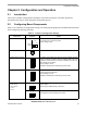
2.3 Operation
This section describes how the system functions and how to use the boards.
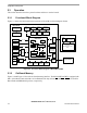
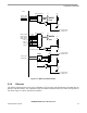
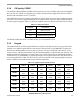
2.3.1 Functional Block Diagram
Figure 2-3 shows the functional interconnections of the ADS in a block diagram format.
Figure 2-3. Functional Block Diagram of M9328MX21ADSE
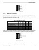
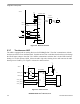
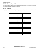
2.3.2 On-Board Memory
Figure 2-4 and Figure 2-5 show the on-board memory interface. The M9328MX21ADSE is equipped with
8M x 32-bit Burst Flash and 16M x 32-bit SDRAM. The chip selects CS0
and CS2 (CSD0) are used for
Burst Flash and SDRAM chip selects, respectively.
i.MX21
SDRAM
Burst Fl ash
Transceiver
CPU Board
High Speed
Connector s
Base boar d connector s
Addr /Data bus
Addr /Data bus
IO pi ns
Ethernet
port
USB series
mini-AB
connector
UART1,
UART2 &
IrDA
Ext.
UART
LEDs & Buzzer
Boot mode,
UARTs, IrDA
selection
1-wire Interface
Silicon & Board
revision register
S/W readable
DIP switches
Audio
CODEC
UART
controller
Ethernet
controller
USB OTG
Transceiver
IO pi ns , PWM
OWIRE
Peripheral si gnals CSI signal s MMC/SD signal s
LCDC
USBOTG si gnalsAddr /Data BusAddr /Data Bus
UART signals
Decoder & Chip
select logic
Addr/Data Bu s
SSI
Base Board
Power Connector,
Power Switch & fuse
3V regulator, CPU
Reset signal
LCD
connector
Battery Level
Measurement
Emulation
Touch screen
controller
LCD panel
(240x320 pixels) & Touch
screen
White
LED
driver
LCD Board
TFT LCD DC-
DC converter
Keypad
Connector
Keypad Board
KPP
NAND Flash
Connector
Multi-ICE
connector
NFC si gnals
TV
Encoder
connector
I2C
Line In
Speaker
Out
Mic In
MMC/SD
connector
Image sensor
connector
Expansion
Connector 1
Expansion
Connector 2
Peripheral si gnals
2. 5V, 1.8V and
1 .5V r egulator s