
User manual


Chapter 23 Memory Mapping Control (S12XMMCV2)
MC9S12XDP512 Data Sheet, Rev. 2.11
Freescale Semiconductor 909
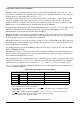
The following conditions must be satisfied to ensure correct operation of the RAM protection mechanism:
• Value stored in RAMXGU must be lower than the value stored in RAMSHL.
• Value stored RAMSHL must be lower or equal than the value stored in RAMSHU.
Figure 23-25. RAM Write Protection Scheme
Table 23-22. RAM Write Protection Interrupt Vectors
Interrupt Source CCR Mask Local Enable
CPU access violation I Bit AVIE in RAMWPC
$0F_FFFF
$00_0000
Shared Region
XGATE RAM
Region
$0F_RAMSHU_FF
$0F_RAMSHL_00
$0F_RAMXGU_FF
Only XGATE is allowed to write
CPU and XGATE are allowed to write
Only CPU is allowed to write
Unimplemented
Only CPU is allowed to write
RAMSIZE
$00_0800
2K Registers