MPC837xE-RDS Reference Design Platform User’s Guide Document Number: MPC837xERDSUG Rev. 1.
How to Reach Us: Home Page: www.freescale.com Web Support: http://www.freescale.com/support USA/Europe or Locations Not Listed: Freescale Semiconductor, Inc. Technical Information Center, EL516 2100 East Elliot Road Tempe, Arizona 85284 1-800-521-6274 or +1-480-768-2130 www.freescale.
Contents About This Book Audience . . . . . . . . . . . . . . . . . . . . . . . . . . . . . . . . . . . . . . . . . . . . . . . . . . . . . . . . . . . . . . . . . . . . Organization . . . . . . . . . . . . . . . . . . . . . . . . . . . . . . . . . . . . . . . . . . . . . . . . . . . . . . . . . . . . . . . . . Definitions, Acronyms, and Abbreviations . . . . . . . . . . . . . . . . . . . . . . . . . . . . . . . . . . . . . . . . . References . . . . . . . . . . . . . . . . . . . . . . . . . . . . . . . . .
2.5.3 2.5.4 2.5.5 2.6 2.7 3 3.1 3.2 4 4.1 4.2 5 5.1 5.2 5.3 Reset Configuration Word . . . . . . . . . . . . . . . . . . . . . . . . . . . . . . . . . . . . . . . . . . . . . . . 26 Power Supply . . . . . . . . . . . . . . . . . . . . . . . . . . . . . . . . . . . . . . . . . . . . . . . . . . . . . . . . . 30 Chip-Select Assignments and Memory Map . . . . . . . . . . . . . . . . . . . . . . . . . . . . . . . . . . . . 30 Specifications . . . . . . . . . . . . . . . . . . . . . . . . . . . . . . . . . . .
About This Book This document presents system architecture, board-level functions, external connections, and software features for the MPC837xE-RDS board. It provides guidance of how to operate this product, making it easy for the user to connect with the outside world. The front part of this book focuses primarily on the board and functions. The latter part of the book focuses on the mechanical aspects.
I2C EEPROM JTAG DHCP DNS VLAN NAT PAT RIP VRRP PPPoE IGMP UPnP SNMP QoS IPsec PPTP L2TP Inter-Integrated Circuit (computer bus) Electrically Erasable Programmable Read-Only Memory Joint Test Action Group Dynamic Host Configuration Protocol Domain Name System Virtual Local Area Networks Network Address Translation Port Address Translation Routing Information Protocol Virtual Router Redundancy Protocol Point-to-Point Protocol over Ethernet Internet Group Management Protocol Universal Plug and Play (computer
Introduction 1 Introduction This section presents the features and block diagram for the MPC837xE-RDS board. 1.1 Overview The MPC837xE-RDS is a reference design based on the MPC8377E PowerQUICCTMII Pro processor. It supports applications of Wi-Fi Router, DMS (Digital Media Server), NAS with RAID, or Office in BOX, etc. The documentation for manufacturing the MPC837xE-RDS—including schematic, Gerber files, reference software, Bill Of Material (BOM)—is on the product CD.
Introduction • • • – Two standard External SATA connectors — PCI: 32-bit PCI interface up to 66 Mhz – 2x 32-bit 3.
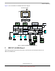
MPC837xE-RDS Board Figure 1 shows the MPC837xE-RDS board block diagram. 48V PoE 48V AC/DC PoE Card LM5072 5V 3.3V 1.8 EEPROM 1.5 1.
MPC837xE-RDS Board 2.1 Board-Level Functions The board-level functions discussed in this section are reset, interrupts, clock distribution, and interface specification. 2.1.1 Reset and Reset Configurations The MPC837xE-RDS reset module generates a single reset to reset the MPC837xE and other peripherals on the board. The reset unit provides power-on reset, hard reset, and soft reset signals in compliance with the MPC837xE hardware specification. Figure 2 shows the reset circuitry.
MPC837xE-RDS Board • 2.1.2 The COP/JTAG port also generates the soft reset for the system. Assertion of SRESET causes the MPC837xE to abort all current internal and external transactions and set most registers to their default values. External Interrupts Figure 3 shows the external interrupt circuitry to the MPC837xE. External Logic IRQ0 TSEC1_IRQ IRQ1 TSEC2_IRQ IRQ2 IRQ3 SD_WP IRQ4 PCI_INTA IRQ5 PCI_INTB IRQ6 IRQ7 MPC837xE Figure 3.
MPC837xE-RDS Board 2.1.3 Clock Distribution Figure 4 and Table 1 show the clock distribution on the MPC837xE-RDS board. 66.
MPC837xE-RDS Board Table 1. Clock Distribution Clock Frequency Module Generated by Description 66.666 MHz MPC837xE CLKIN 66.666 MHz oscillator The MPC837xE uses CLKIN to generate the PCI_SYNC_OUT clock signal, which is fed back to the internal system PLL through the PCI_SYNC_IN signal. From the power-on reset configuration, the internal PLL generates the CSB clock, which is fed to the e300 core PLL for generating the e300 core clock.
MPC837xE-RDS Board MPC837xE DQ[0:63] DM[0:7] DQS[0:7] DQ[0:15] DQ[16:31] DM[0,1] DM[2,3] DQS[0,1] A[0:12], BA[0:2],CTRL DDR2 SDRAM 1Gb(X16) DQS[2,3] Vref MCK0 pair MCK1 pair DQ[32:47] DQ[48:63] DDR2 SDRAM 1Gb(X16) Vref DDR2 SDRAM Controller DM[4,5] MSYNC_OUT DQS[4,5] MSYNC_IN DDR2 SDRAM 1Gb(X16) Vref DQS[6,7] 1.8 V Input Vref 0.9 V DDR2 SDRAM 1Gb(X16) Vref MCK3 pair MCK2 pair MCK[0:3] pairs DM[6,7] Vref Generator Vref Figure 5. DDR2 SDRAM Connection 2.1.
MPC837xE-RDS Board Figure 6 shows the block diagram and connections for the local bus. MPC837xE Local Bus Controller LCS0 LCS0 LAD[0:31] LAD[6:26] NOR Flash (16-bit) A[6:30] Address Latch BADDR[27:30] LE LALE OE LAD[0:15] D[0:15] LCS0 GND Control Signals A[24:0] D[15:0] CS Control Control LCLK1 LCLK0 LSYNC_IN LCKE LSYNC_OUT S29GL512N Figure 6. Local Bus Connections 2.1.6 Flash Memory MPC837xE-RDS provides 64Mbytes NOR Flash memory using general-purpose chip-select machine (GPCM).
MPC837xE-RDS Board 2.1.8 SATA Controller MPC837xE has a SATA controller for storage applications as shown in Figure 7. There are two SATA channels for MPC8377E. It requires a 100-MHz input clock, which is provided by the clock generator. 2.1.9 PCI Express Interface (PCI-E & Mini PCI-E) MPC8377E supports the PCI Express (PCI-E) interface. It can be configured as two mini PCI-E interfaces or one mini PCI-E interface and one 1X PCI-E interface as shown in Figure 7.
MPC837xE-RDS Board the RTL8211B. Figure 8 shows the connection between the MPC837xE eTSEC1 and eTSEC2 to the RTL8211B. MPC837xE PHY addr = 0x02 RTL8211B eTSEC1 RGMII interface EC_MDIO EC_MDC 3.3 V MDIO MDC RJ-45 (Enet0, supports PoE) LVDD1 eTSEC2 RGMII interface PHY addr = 0x03 RTL8211B 3.3 V RJ-45 (Enet1) MDIO MDC LVDD2 Figure 8. RGMII Interface Connection for 10/100/1000 BaseT Ethernet 2.1.11 RS-232 Port Figure 9 illustrates the serial port connection using a SP3232 3.
MPC837xE-RDS Board USB3300 PHY connects to a Type A receptacle connector that serves as a host interface. Figure 10 shows the connection of USB. MPC837xE USB3300 5V D[7:0] DIR STP NXT CLKOUT ULPI_D[7:0] ULPI_DIR ULPI_STP ULPI_NXT ULPI_CLK VBUS ID USB_TYPE_A_RECEPTACLE DM DP Figure 10. USB Port Connections 2.1.13 PCI Subsystem The MPC837xE has PCI interfaces. It connects to two 32-bit 3.3 V mini PCI slots, as shown in Figure 11. MPC837xE PCI-AD[0:31] PCI-CBE[0:3] AD15 32-Bit 3.
MPC837xE-RDS Board Ethernet port, USB port, parallel port, RS-232, etc. Figure 12 shows a typical setup using a USB port emulator. PC J4 USB Emulator MPC837xE-RDS Figure 12. Connecting the MPC837xE-RDS Board to a Parallel Emulator The 16-pin generic header connector carries the COP/JTAG signals and the additional signals for system debugging. Figure 13 shows the connector pinout. 1 TDO GND TDI TRST Pull-up Pull-up TCK NC TMS NC SRESET NC HRESET NC CKSTP_OUT GND Figure 13.
MPC837xE-RDS Board 2.2 MPC837xE-RDS Assembly Figure 14 shows the MPC837xE-RDS board top view, with the references of LEDs, jumpers, headers, and switches. J15 JP1 J4 COP Connector Pin 1 J14 J13 48 V DC Power P1 WAN (supports PoE) MPC837xE P5 Mini PCI-E D7 D8 D9 P2 LAN D11 J12 D14 J16 eSATA P3 Mini PCI (Top) D15 P4 Mini PCI (Bottom) P6 Mini PCI-E J7 SW1 Reset J5 USB Pin 1 J6 J10 RS232 COM1 P7 PCI-E (1x) Figure 14. MPC837xE-RDS Top View CAUTION Use 3.
MPC837xE-RDS Board Figure 15 shows the MPC837xE-RDS board bottom view. J11 SD Socket Figure 15. MPC837xE-RDS Bottom View Table 2 shows references and descriptions of LEDs, jumpers, headers, and switches. Table 2. Lists of Connectors, Jumpers, Switches, and LEDs Reference Description Connectors J4 16-pin COP/JTAG connector MPC837xE-RDS, Rev. 1.
MPC837xE-RDS Board Table 2. Lists of Connectors, Jumpers, Switches, and LEDs (continued) Reference P3, P4 Description 32-bit 3.3 V mini PCI connector slots. The board supports up to 2 mini PCI devices.
MPC837xE-RDS Board Table 3. COP Connector Pin Assignments 2.3.2 Pin Signal Pin Signal 9 TMS 10 NC 11 SRESET 12 NC 13 HRESET 14 NC 15 CHKSTOP_OUT 16 GND RS-232C Connectors Serial interface COM1 is available at connector (J6) with pin assignments as shown in Table 4. Table 4. COM1 Connector Pins 2.3.
MPC837xE-RDS Board Mini PC I Card 1. Insert the card 2. Press downward Figure 16. Installation of a Mini PCI Card 2.3.5 Power Connector J13 is a DC jack for a 48 V power supply to the MPC837xE-RDS board. 2.4 LEDs Figure 17 shows 9 LED indicators on the front panel of MPC837xE-RDS. LAN WAN POWER WiFi DIAG 1000 100 10 Figure 17. LED Indicators on the Front Panel of MPC837xE-RDS 2.4.1 Power-on LED Green Power LED (D15): indicates the system is power-on if lit. 2.4.
MPC837xE-RDS Board 2.4.3 Ethernet LEDs Green Link1000 LEDs (D9): indicate the link speed is 1000M on WAN and LAN. (The top LED for LAN and the bottom one for WAN) Green Link100 LEDs (D8): indicate the link speed is 100M on WAN and LAN. (The top LED for LAN and the bottom one for WAN) Green Link10 LEDs (D7): indicate the link speed is 10M on WAN and LAN. (The top LED for LAN and the bottom one for WAN) 2.
MPC837xE-RDS Board 2.5.3 Reset Configuration Word The reset configuration word (RCW) controls the clock ratios and other basic device functions, such as PCI host or agent mode, boot location, TSEC modes, and endian mode. The reset configuration word is divided into reset configuration word lower (RCWL) and reset configuration word higher (RCWH) and is loaded from the local bus during the power-on or hard reset flow. The default RCW low-bit setting is 0x0404_0000.
MPC837xE-RDS Board Table 6. RCWL Bit Descriptions (continued) Bits Name 2–3 — 4–7 SPMF[0–3] 4–7 SPMF[0–3] 8 — 9–15 COREPLL [0–6] Meaning Reserved Description Should be cleared. System PLL 0000 multiplication factor 0001 16:1 Reserved 0010 2:1 0011 3:1 0100 (default) 4:1 0101 5:1 System PLL 0110 multiplication factor 0111 6:1 7:1 1000 8:1 1001 9:1 1010 10:1 1011 11:1 1100 12:1 1101 13:1 1110 14:1 1111 15:1 Reserved Should be cleared.
MPC837xE-RDS Board Table 6. RCWL Bit Descriptions (continued) Bits Name 9–15 COREPLL [0–6] 16–31 Meaning — Description 01 0010 0 2:1 4 10 0010 0 2:1 8 11 0010 0 2:1 8 00 0010 1 2.5:1 2 01 0010 1 2.5:1 4 10 0010 1 2.5:1 8 11 0010 1 2.5:1 8 00 0011 0 3:1 2 01 0011 0 3:1 4 10 0011 0 3:1 8 11 0011 0 3:1 8 Reserved. Should be cleared. Table 7.
MPC837xE-RDS Board Table 7.
MPC837xE-RDS Board Table 7. Reset Configuration Word High (RCWH) Bit Descriptions (continued) Bits Name Meaning 30 LDP LDP/CKSTP pin mux state after reset 0 LDP[0:3] = local data parity. 1: Default LDP[0:3] = LCS[4:7] — Should be cleared 31 2.5.4 Reserved Detailed Description Power Supply The MPC837xE requires a 48 V power supply from the DC power jack or PoE for normal operation. The 48 V power supply is reduced to 5 V and 3.3 V from the DC-DC circuitry on PoE daughter board. The 1.
MPC837xE-RDS Board Table 9. MPC837xE-RDS Board Specifications (continued) Characteristics Specifications Addressing: Total address range Flash memory (local bus) DDR SDRAM 4 Gbyte (32 address lines) 64 Mbyte NOR Flash 512 Mbyte DDR2 SDRAM at DDR400 Operating temperature 0oC to 70oC (room temperature) Storage temperature –25oC to 85oC Relative humidity 5% to 90% (noncondensing) PCB dimensions: Length Width Thickness 6693 mil 6693 mil 67 mil MPC837xE-RDS, Rev. 1.
Board Bootup 2.7 Mechanical Data Figure 21 shows the MPC837xE-RDS dimensions (in mil). The board dimensions are 170 mm × 170 mm (6693 mils × 6693 mils) for integration in a mini ITX chassis with a small footprint. 2590.00 2060.00 mounting hole typ 4 1360.00 6693.00 6693.00 Figure 21. Dimensions of the MPC837xE-RDS Board 3 Board Bootup This section describes how to boot up the MPC837xE-RDS board. The factory has preloaded a Flash image onto the on-board Flash memory.
Board Bootup CAUTION Avoid touching areas of circuitry and connectors; static discharge can damage circuits. 3.1 Board Jumper Settings Figure 22 shows a partial top view of the MPC837xE-RDS with red outlines at jumper designators J7, J10, and J12. A square pad indicates pin 1 of the part. Table 10 shows the default jumper settings. Figure 22. Partial MPC837xE-RDS Top View Table 10. Default Jumper Settings √ = Jumper × = No Jumper Description J7 × Watchdog input for MAX6829. Default is no jumper.
MPC837xE-RDS Software 3.2 External Connections Figure 23shows the external connections. SD Card 48V Power WAN LAN (Support PoE) eSATA Reset USB Figure 23. External Connections NOTE Strong electromagnetic interference might disturb the normal function of the product. If so, simply reset the product to resume normal operation by following the steps in the software user guide. If normal function does not return, please move the product to another location.
MPC837xE-RDS Software • • • • • PPPoE IGMP UPnP SNMP QoS Wireless Security: • Pre-Shared Key (PSK) • Wi-Fi Protected Access 2 (WPA2) • 802.11i AES-CCMP • Wired Equivalent Privacy (WEP), 128/256-bit • 802.11i EAP authentication with RADIUS Network Security: • Access control • Stateful packet inspection firewall • Intrusion detection • Content filtering Virtual Private Network (VPN): • IPSec • PPTP • L2TP MPC837xE-RDS, Rev. 1.
MPC837xE-RDS Software 4.2 Application Connections Figure 24 shows application connections for MPC837xE-RDS board. Figure 24. MPC837xE-RDS Application Connections Configure the MPC837xE-RDS board by using a web browser. Connect your PC to the LAN port of the board (either directly or through a hub), then use a web browser to configure. TCP/IP settings must be correct. The TCP/IP setting should be on the IP subnet of the MPC837xE-RDS.
Unit Assembly 5 Unit Assembly The assembled unit is composed of the board assembly, an enclosure, screws, and other parts. The instructions in this section apply if you need to assemble or reassemble the product or add peripherals mentioned. 5.1 Assembling the Enclosure and Board Assembly Assembling the board into the enclosure requires screwing the board onto the base, then screwing the top and base together. 1. Place the base on a flat surface. 2.
Unit Assembly 5. Re-assemble using Steps 2 through 5 of Section 5.1, Assembling the Enclosure and Board Assembly. MPC837xE-RDS, Rev. 1.