
User's Guide
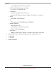
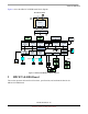
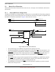
Table Of Contents
- About This Book
- 1 Introduction
- 2 MPC837xE-RDS Board
- 2.1 Board-Level Functions
- 2.1.1 Reset and Reset Configurations
- 2.1.2 External Interrupts
- 2.1.3 Clock Distribution
- 2.1.4 DDR2 SDRAM Controller
- 2.1.5 Local Bus Controller
- 2.1.6 Flash Memory
- 2.1.7 I2C
- 2.1.8 SATA Controller
- 2.1.9 PCI Express Interface (PCI-E & Mini PCI-E)
- 2.1.10 10/100/1000 BaseT Interface
- 2.1.11 RS-232 Port
- 2.1.12 USB 2.0 Interface
- 2.1.13 PCI Subsystem
- 2.1.14 COP/JTAG Port
- 2.2 MPC837xE-RDS Assembly
- 2.3 Connectors
- 2.4 LEDs
- 2.5 MPC837xE-RDS Board Configuration
- 2.6 Specifications
- 2.7 Mechanical Data
- 2.1 Board-Level Functions
- 3 Board Bootup
- 4 MPC837xE-RDS Software
- 5 Unit Assembly
- MPC837xE-RDS

MPC837xE-RDS, Rev. 1.0
10 Freescale Semiconductor
Preliminary, Subject to Change without Notice
MPC837xE-RDS Board
2.1 Board-Level Functions
The board-level functions discussed in this section are reset, interrupts, clock distribution, and interface
specification.
2.1.1 Reset and Reset Configurations
The MPC837xE-RDS reset module generates a single reset to reset the MPC837xE and other peripherals
on the board. The reset unit provides power-on reset, hard reset, and soft reset signals in compliance with
the MPC837xE hardware specification. Figure 2 shows the reset circuitry.
Figure 2. Reset Circuitry of the MPC837xE
• The COP/JTAG port or the MPC837xE generates the signal for hard reset.
• The Maxim MAX6829 device generates the power-on reset. When MR is de-asserted and 3.3 V is
ready, the MAX6829 internal timeout guarantees a minimum reset active time of 140 ms before
PORESET is de-asserted. This circuitry guarantees a 140 ms PORESET pulse width after 3.3 V
reaches the right voltage level, and this meets the specification of the PORESET
input of
MPC837xE.
• The COP/JTAG port reset provides convenient hard-reset capability for a COP/JTAG controller.
The RESET line is available at the COP/JTAG port connector. The COP/JTAG controller can
directly generate the hard-reset signal by asserting this line low.
• The pushbutton reset interfaces the MR
signal with a debounce capability to produce a manual
master reset of the processor.
MAX6829
3.3 V
Push Button
HRESET from COP
SRESET
from COP
TRST
from COP
SRESET
to MPC837xE
PORESET
to MPC837xE
FLASH
10/100/1000 PHY
MPC837xE
TRST to MPC837xE
GND
1.0 V
MR
Watchdog Input from MPC837xE
PCI-E & Mini PCI-E