
User's Guide
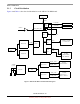
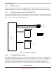
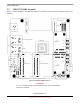
Table Of Contents
- About This Book
- 1 Introduction
- 2 MPC837xE-RDS Board
- 2.1 Board-Level Functions
- 2.1.1 Reset and Reset Configurations
- 2.1.2 External Interrupts
- 2.1.3 Clock Distribution
- 2.1.4 DDR2 SDRAM Controller
- 2.1.5 Local Bus Controller
- 2.1.6 Flash Memory
- 2.1.7 I2C
- 2.1.8 SATA Controller
- 2.1.9 PCI Express Interface (PCI-E & Mini PCI-E)
- 2.1.10 10/100/1000 BaseT Interface
- 2.1.11 RS-232 Port
- 2.1.12 USB 2.0 Interface
- 2.1.13 PCI Subsystem
- 2.1.14 COP/JTAG Port
- 2.2 MPC837xE-RDS Assembly
- 2.3 Connectors
- 2.4 LEDs
- 2.5 MPC837xE-RDS Board Configuration
- 2.6 Specifications
- 2.7 Mechanical Data
- 2.1 Board-Level Functions
- 3 Board Bootup
- 4 MPC837xE-RDS Software
- 5 Unit Assembly
- MPC837xE-RDS

MPC837xE-RDS Board
MPC837xE-RDS, Rev. 1.0
Freescale Semiconductor 11
Preliminary, Subject to Change without Notice
• The COP/JTAG port also generates the soft reset for the system. Assertion of SRESET causes the
MPC837xE to abort all current internal and external transactions and set most registers to their
default values.
2.1.2 External Interrupts
Figure 3 shows the external interrupt circuitry to the MPC837xE.
Figure 3. MPC837xE Interrupt Circuitry
The following items describe the interrupt signals shown in Figure 3:
• PHY interrupt (TSEC1_IRQ, TSEC2_IRQ). Two RTL8211B GBE PHY interrupts are connected
to IRQ1 and IRQ2 of the MPC837xE. The system software can detect the status of the Ethernet
link and the PHY internal status.
• SD Card Write Protect interrupt (SD_WP). The SD card socket has a mechanical pin that can
indicate whether the SD card inserted is write-protected or not. It is connected to IRQ4
of the
MPC837xE.
• PCI interrupt (PCI_INTA
, PCI_INTB). Two mini PCI slots INTA and INTB drive IRQ5 and IRQ6
of the MPC837xE, respectively
TSEC1_IRQ
SD_WP
PCI_INTA
PCI_INTB
IRQ1
IRQ2
IRQ3
IRQ4
IRQ5
IRQ6
IRQ7
MPC837xE
External Logic
IRQ0
TSEC2_IRQ