
User's Guide
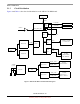
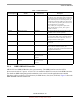
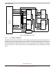
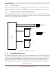
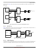
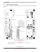
Table Of Contents
- About This Book
- 1 Introduction
- 2 MPC837xE-RDS Board
- 2.1 Board-Level Functions
- 2.1.1 Reset and Reset Configurations
- 2.1.2 External Interrupts
- 2.1.3 Clock Distribution
- 2.1.4 DDR2 SDRAM Controller
- 2.1.5 Local Bus Controller
- 2.1.6 Flash Memory
- 2.1.7 I2C
- 2.1.8 SATA Controller
- 2.1.9 PCI Express Interface (PCI-E & Mini PCI-E)
- 2.1.10 10/100/1000 BaseT Interface
- 2.1.11 RS-232 Port
- 2.1.12 USB 2.0 Interface
- 2.1.13 PCI Subsystem
- 2.1.14 COP/JTAG Port
- 2.2 MPC837xE-RDS Assembly
- 2.3 Connectors
- 2.4 LEDs
- 2.5 MPC837xE-RDS Board Configuration
- 2.6 Specifications
- 2.7 Mechanical Data
- 2.1 Board-Level Functions
- 3 Board Bootup
- 4 MPC837xE-RDS Software
- 5 Unit Assembly
- MPC837xE-RDS

MPC837xE-RDS Board
MPC837xE-RDS, Rev. 1.0
Freescale Semiconductor 13
Preliminary, Subject to Change without Notice
2.1.4 DDR2 SDRAM Controller
MPC837xE uses DDR2 SDRAM as the system memory. The DDR2 interface uses the SSTL2
driver/receiver and 1.8 V power. A Vref 1.8V/2 is needed for all SSTL2 receivers in the DDR2 interface.
For details on DDR timing design and termination, refer to the Freescale application note entitled
Hardware and Layout Design Considerations for DDR Memory Interfaces (AN2582). Figure 5 shows the
DDR SDRAM controller connection.
Table 1. Clock Distribution
Clock Frequency Module Generated by Description
66.666 MHz MPC837xE CLKIN 66.666 MHz oscillator The MPC837xE uses CLKIN to generate the
PCI_SYNC_OUT clock signal, which is fed back to
the internal system PLL through the PCI_SYNC_IN
signal. From the power-on reset configuration, the
internal PLL generates the CSB clock, which is fed to
the e300 core PLL for generating the e300 core clock.
The PCI M66EN pin is inverted for
CFG_CLKIN_DIV configuration input, which
selects whether the PCI_SYNC_OUT signal is
CLKIN or CLkIN/2.
125 MHz MPC837xE eTSEC RTL8211B The gigabit Ethernet PHY (RTL8211B) provides a
125-MHZ clock for eTSEC operation.)
200 MHz DDR2 SDRAM MPC837xE The DDR memory controller is configured to use the
1:1 mode CSB to DDR clock for the DDR interface.
The local bus clock uses CCB/n clock, where n is
configured from the LCRR register.
25 MHz GBE PHY (RTL8211B) 25 MHz oscillator The 25 MHz oscillator generates the clock for
RTL8211B.
33/66 MHz Mini PCI slot MPC837xE The PCI module uses the PCI_SYNC_IN as its clock
source. The trace of the PCI_SYNC_IN/
PCI_SYNC_OUT signal is synchronized with all the
PCI signals of the PCI slots.
24 MHz USB PHY (USB3300) 24 MHz crystal
100 MHz SerDes Interface 25 MHz oscillator and
PI6C557-03 clock
generator
The SerDes reference clock uses 100 MHz.
100 MHz Mini PCI-e and PCI-e x1
Interface
25 MHz oscillator and
PI6C557-03 clock
generator