
User's Guide
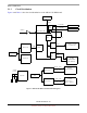
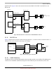
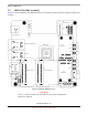
Table Of Contents
- About This Book
- 1 Introduction
- 2 MPC837xE-RDS Board
- 2.1 Board-Level Functions
- 2.1.1 Reset and Reset Configurations
- 2.1.2 External Interrupts
- 2.1.3 Clock Distribution
- 2.1.4 DDR2 SDRAM Controller
- 2.1.5 Local Bus Controller
- 2.1.6 Flash Memory
- 2.1.7 I2C
- 2.1.8 SATA Controller
- 2.1.9 PCI Express Interface (PCI-E & Mini PCI-E)
- 2.1.10 10/100/1000 BaseT Interface
- 2.1.11 RS-232 Port
- 2.1.12 USB 2.0 Interface
- 2.1.13 PCI Subsystem
- 2.1.14 COP/JTAG Port
- 2.2 MPC837xE-RDS Assembly
- 2.3 Connectors
- 2.4 LEDs
- 2.5 MPC837xE-RDS Board Configuration
- 2.6 Specifications
- 2.7 Mechanical Data
- 2.1 Board-Level Functions
- 3 Board Bootup
- 4 MPC837xE-RDS Software
- 5 Unit Assembly
- MPC837xE-RDS

MPC837xE-RDS, Rev. 1.0
14 Freescale Semiconductor
Preliminary, Subject to Change without Notice
MPC837xE-RDS Board
Figure 5. DDR2 SDRAM Connection
2.1.5 Local Bus Controller
The MPC837xE local bus controller has a 32-bit LAD[0–31] address that consists of data multiplex bus
and control signals. The local bus speed is up to 133 MHz. To interface with the standard memory device,
an address latch must provide the address signals. The LALE is used as the latching signal. To reduce the
load of the high speed 32-bit local bus interface, there is a data buffer for all low-speed devices attached
to the memory controller. The local bus only drives the 64MB NOR Flash menory on the MPC837xE-RDS
board:
DDR2
SDRAM
Controller
Vref
Generator
Vref 0.9 V
1.8 V Input
Vref
MSYNC_OUT
MSYNC_IN
MPC837xE
DDR2
SDRAM
Vref
Vref
DQ[0:63]
DQ[32:47]
DQ[0:15]
DM[0:7]
DM[0,1]
DM[4,5]
DQS[0:7]
DQS[0,1]
DQS[4,5]
A[0:12], BA[0:2],CTRL
MCK[0:3] pairs
MCK0
MCK2 pair
DDR2
SDRAM
DDR2
SDRAM
DQ[48:63]
DQ[16:31]
DM[2,3]
DM[6,7]
DQS[2,3]
DQS[6,7]
MCK1 pair
MCK3 pair
DDR2
SDRAM
Vref
Vref
1Gb(X16)
1Gb(X16)
1Gb(X16)
1Gb(X16)
pair