
User's Guide
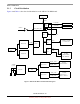
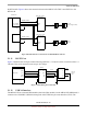
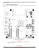
Table Of Contents
- About This Book
- 1 Introduction
- 2 MPC837xE-RDS Board
- 2.1 Board-Level Functions
- 2.1.1 Reset and Reset Configurations
- 2.1.2 External Interrupts
- 2.1.3 Clock Distribution
- 2.1.4 DDR2 SDRAM Controller
- 2.1.5 Local Bus Controller
- 2.1.6 Flash Memory
- 2.1.7 I2C
- 2.1.8 SATA Controller
- 2.1.9 PCI Express Interface (PCI-E & Mini PCI-E)
- 2.1.10 10/100/1000 BaseT Interface
- 2.1.11 RS-232 Port
- 2.1.12 USB 2.0 Interface
- 2.1.13 PCI Subsystem
- 2.1.14 COP/JTAG Port
- 2.2 MPC837xE-RDS Assembly
- 2.3 Connectors
- 2.4 LEDs
- 2.5 MPC837xE-RDS Board Configuration
- 2.6 Specifications
- 2.7 Mechanical Data
- 2.1 Board-Level Functions
- 3 Board Bootup
- 4 MPC837xE-RDS Software
- 5 Unit Assembly
- MPC837xE-RDS

MPC837xE-RDS Board
MPC837xE-RDS, Rev. 1.0
Freescale Semiconductor 15
Preliminary, Subject to Change without Notice
Figure 6 shows the block diagram and connections for the local bus.
Figure 6. Local Bus Connections
2.1.6 Flash Memory
MPC837xE-RDS provides 64Mbytes NOR Flash memory using general-purpose chip-select machine
(GPCM). The NOR Flash is 16-bit port size in the system. It is selected as the boot Flash when J12 pins 2
and 3 are jumpered together.
2.1.7 I
2
C
The MPC837xE has two I
2
C interfaces. On the MPC837xE-RDS board, the MPC837xE serves as I
2
C
master for both I
2
C buses (I2C1 and I2C2). I2C1 is connected to the following:
• Serial EEPROM M24256 at address 0x50.
• PCI-E and mini PCI-E socket.
The M24256 serial EEPROM can store the reset configuration word of the MPC837xE, as well as store
the configuration registers values if the boot sequencer of MPC837xE is enabled. The I
2
C address of the
M24256 EEPROM on I2C1 bus is 0x50.
A[24:0]
CS
S29GL512N
NOR Flash (16-bit)
MPC837xE
LAD[0:31]
BADDR[27:30]
D[15:0]
LALE
Address
LE
Local Bus
LCS0
Control
OE
D[0:15]
A[6:30]
LCS0
Latch
LCS0
Control
LAD[6:26]
LAD[0:15]
Controller
GND
Control Signals
LSYNC_OUT
LSYNC_IN
LCKE
LCLK0
LCLK1