
User's Guide
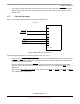
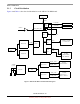
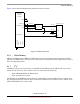
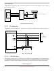
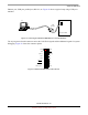
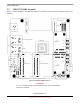
Table Of Contents
- About This Book
- 1 Introduction
- 2 MPC837xE-RDS Board
- 2.1 Board-Level Functions
- 2.1.1 Reset and Reset Configurations
- 2.1.2 External Interrupts
- 2.1.3 Clock Distribution
- 2.1.4 DDR2 SDRAM Controller
- 2.1.5 Local Bus Controller
- 2.1.6 Flash Memory
- 2.1.7 I2C
- 2.1.8 SATA Controller
- 2.1.9 PCI Express Interface (PCI-E & Mini PCI-E)
- 2.1.10 10/100/1000 BaseT Interface
- 2.1.11 RS-232 Port
- 2.1.12 USB 2.0 Interface
- 2.1.13 PCI Subsystem
- 2.1.14 COP/JTAG Port
- 2.2 MPC837xE-RDS Assembly
- 2.3 Connectors
- 2.4 LEDs
- 2.5 MPC837xE-RDS Board Configuration
- 2.6 Specifications
- 2.7 Mechanical Data
- 2.1 Board-Level Functions
- 3 Board Bootup
- 4 MPC837xE-RDS Software
- 5 Unit Assembly
- MPC837xE-RDS

MPC837xE-RDS Board
MPC837xE-RDS, Rev. 1.0
Freescale Semiconductor 19
Preliminary, Subject to Change without Notice
Ethernet port, USB port, parallel port, RS-232, etc. Figure 12 shows a typical setup using a USB port
emulator.
Figure 12. Connecting the MPC837xE-RDS Board to a Parallel Emulator
The 16-pin generic header connector carries the COP/JTAG signals and the additional signals for system
debugging. Figure 13 shows the connector pinout.
Figure 13. MPC837xE-RDS Board COP Connector
PC
MPC837xE-RDS
J4
USB
Emulator
TDI
Pull-up
TCK
TMS
SRESET
HRESET
CKSTP_OUT
GND
TRST
Pull-up
NC
NC
GND
1
TDO
NC
NC