
User's Guide
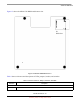
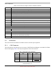
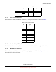
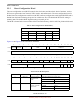
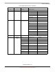
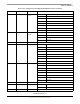
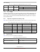
Table Of Contents
- About This Book
- 1 Introduction
- 2 MPC837xE-RDS Board
- 2.1 Board-Level Functions
- 2.1.1 Reset and Reset Configurations
- 2.1.2 External Interrupts
- 2.1.3 Clock Distribution
- 2.1.4 DDR2 SDRAM Controller
- 2.1.5 Local Bus Controller
- 2.1.6 Flash Memory
- 2.1.7 I2C
- 2.1.8 SATA Controller
- 2.1.9 PCI Express Interface (PCI-E & Mini PCI-E)
- 2.1.10 10/100/1000 BaseT Interface
- 2.1.11 RS-232 Port
- 2.1.12 USB 2.0 Interface
- 2.1.13 PCI Subsystem
- 2.1.14 COP/JTAG Port
- 2.2 MPC837xE-RDS Assembly
- 2.3 Connectors
- 2.4 LEDs
- 2.5 MPC837xE-RDS Board Configuration
- 2.6 Specifications
- 2.7 Mechanical Data
- 2.1 Board-Level Functions
- 3 Board Bootup
- 4 MPC837xE-RDS Software
- 5 Unit Assembly
- MPC837xE-RDS

MPC837xE-RDS, Rev. 1.0
22 Freescale Semiconductor
Preliminary, Subject to Change without Notice
MPC837xE-RDS Board
2.3 Connectors
This section describes the MPC837xE-RDS connectors and their pin assignments.
2.3.1 COP Connector
The COP connector (J4) allows the user to connect a COP/JTAG-based debugger to the MPC837xE-RDS
board for debugging. Table 3 lists the pin assignments of the COP connector.
P3, P4 32-bit 3.3 V mini PCI connector slots. The board supports up to 2 mini PCI devices.
J5 USB Type A receptacle (for USB high-speed external device)
J13 48 V DC power jack (external power adapter input)
J16 Double-eSATA port
J6 COM1 serial port terminal connector (RS-232C) for MPC837xE
P5, P6 Mini PCI-E connectors
P7 PCI-E (1X) connector
P1 RJ-45 connector Enet0 (GBit Ethernet port that connects to Ethernet Switch). Enet0 is the WAN connector and supports
PoE.
P2 RJ-45 connector Enet1 (GBit Ethernet port that connects to external device). Enet1 is the LAN connector.
J11 SD Card socket
Jumpers (Refer to Table 1 0 )
Switches
SW1 System reset button. Resets the MPC837xE-RDS board.
LEDs (See also Section 2.4, LEDs)
D11, D14 Controlled by the GPIO pin of MPC837xE.
D7, D8, D9 eTSEC1 Eth0 link10, link100, link1000 LEDs (top)
eTSEC2 Eth1 lind10, link100, link1000 LEDs (bottom)
D15 3.3 V Active (Power is on if lit, and 3.3 V power is good.)
Table 3. COP Connector Pin Assignments
Pin Signal Pin Signal
1 TDO 2 GND
3TDI 4TRST
5QREQ 6 VDD_SENSE
7 TCK 8 CHKSTOP_IN
Table 2. Lists of Connectors, Jumpers, Switches, and LEDs (continued)
Reference Description