
User's Guide
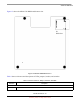
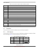
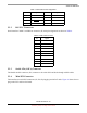
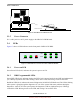
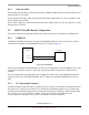
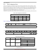
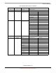
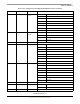
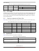
Table Of Contents
- About This Book
- 1 Introduction
- 2 MPC837xE-RDS Board
- 2.1 Board-Level Functions
- 2.1.1 Reset and Reset Configurations
- 2.1.2 External Interrupts
- 2.1.3 Clock Distribution
- 2.1.4 DDR2 SDRAM Controller
- 2.1.5 Local Bus Controller
- 2.1.6 Flash Memory
- 2.1.7 I2C
- 2.1.8 SATA Controller
- 2.1.9 PCI Express Interface (PCI-E & Mini PCI-E)
- 2.1.10 10/100/1000 BaseT Interface
- 2.1.11 RS-232 Port
- 2.1.12 USB 2.0 Interface
- 2.1.13 PCI Subsystem
- 2.1.14 COP/JTAG Port
- 2.2 MPC837xE-RDS Assembly
- 2.3 Connectors
- 2.4 LEDs
- 2.5 MPC837xE-RDS Board Configuration
- 2.6 Specifications
- 2.7 Mechanical Data
- 2.1 Board-Level Functions
- 3 Board Bootup
- 4 MPC837xE-RDS Software
- 5 Unit Assembly
- MPC837xE-RDS

MPC837xE-RDS Board
MPC837xE-RDS, Rev. 1.0
Freescale Semiconductor 23
Preliminary, Subject to Change without Notice
2.3.2 RS-232C Connectors
Serial interface COM1 is available at connector (J6) with pin assignments as shown in Table 4.
2.3.3 Serial ATA (SATA) Connector
The Double-eSATA connector (J16) connects to the serial ATA hard disks through eSATA cables.
2.3.4 Mini PCI Connector
The board has two mini-PCI connectors (P3, P4) for plugging in mini PCI cards. Figure 16 shows how to
plug a mini PCI card into the board.
9TMS 10 NC
11 SRESET
12 NC
13 HRESET
14 NC
15 CHKSTOP_OUT 16 GND
Table 4. COM1 Connector Pins
Pin Signal
1 GND
2
TXD
3
RXD
4
NC
5
GND
6 GND
7CTS
8RTS
9NC
10 NC
Table 3. COP Connector Pin Assignments
Pin Signal Pin Signal