
User's Guide
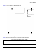
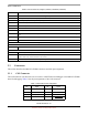
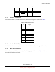
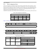
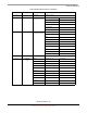
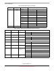
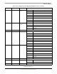
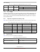
Table Of Contents
- About This Book
- 1 Introduction
- 2 MPC837xE-RDS Board
- 2.1 Board-Level Functions
- 2.1.1 Reset and Reset Configurations
- 2.1.2 External Interrupts
- 2.1.3 Clock Distribution
- 2.1.4 DDR2 SDRAM Controller
- 2.1.5 Local Bus Controller
- 2.1.6 Flash Memory
- 2.1.7 I2C
- 2.1.8 SATA Controller
- 2.1.9 PCI Express Interface (PCI-E & Mini PCI-E)
- 2.1.10 10/100/1000 BaseT Interface
- 2.1.11 RS-232 Port
- 2.1.12 USB 2.0 Interface
- 2.1.13 PCI Subsystem
- 2.1.14 COP/JTAG Port
- 2.2 MPC837xE-RDS Assembly
- 2.3 Connectors
- 2.4 LEDs
- 2.5 MPC837xE-RDS Board Configuration
- 2.6 Specifications
- 2.7 Mechanical Data
- 2.1 Board-Level Functions
- 3 Board Bootup
- 4 MPC837xE-RDS Software
- 5 Unit Assembly
- MPC837xE-RDS

MPC837xE-RDS, Rev. 1.0
26 Freescale Semiconductor
Preliminary, Subject to Change without Notice
MPC837xE-RDS Board
2.5.3 Reset Configuration Word
The reset configuration word (RCW) controls the clock ratios and other basic device functions, such as
PCI host or agent mode, boot location, TSEC modes, and endian mode. The reset configuration word is
divided into reset configuration word lower (RCWL) and reset configuration word higher (RCWH) and is
loaded from the local bus during the power-on or hard reset flow. The default RCW low-bit setting is
0x0404_0000. The default RCW high-bit setting is 0xA060_6C02.
The RCW is located at the lowest 64 bits of the boot Flash memory, which is 0xFC00_0000 on this board.
Figure 19 and Figure 20 show the RCW definitions.
Table 5. RCW Configuration in Flash Memory
Address
FC000000: 26262626 26262626 03030303 03030303
FC000010: 00000000 00000000 00000000 00000000
FC000020: A0A0A0A0 A0A0A0A0 60606060 60606060
FC000030: 6C6C6C6C 6C6C6C6C 02020202 02020202
0 1 2 3 4 5 6 7 8 9 10 11 12 13 14 15
Field LBIUCM DDRCM — SPMF — COREPLL
16 17 18 19 20 21 22 23 24 25 26 27 28 29 30 31
Field —
Figure 19. Reset Configuration Word Low (RCWL) Bit Settings
0 1 2 3 4 5 6 7 8 9 10 11 12 13 14 15
Field PCIHOST — PCIABR — COREDIS BMS BOOTSEQ SWEN ROMLOC RLEXT — —
16 17 18 19 20 21 22 23 24 25 26 27 28 29 30 31
Field TSEC1M TSEC2M — TLE — LDP —
Figure 20. Reset Configuration Word High (RCWH) Bit Settings
Table 6. RCWL Bit Descriptions
Bits Name Meaning Description
0 LBIUCM Local bus memory
controller clock
mode
Local Bus Controller Clock: CSB_CLK
0: Default ratio 1:1
1: ratio 2:1
1 DDRCM DDR SDRAM
memory controller
clock mode
DDR Controller Clock: CSB_CLK
0: Default ratio 1:1
1: ratio 2:1