
User's Guide
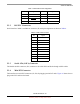
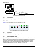
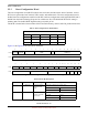
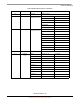
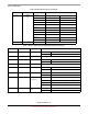
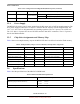
Table Of Contents
- About This Book
- 1 Introduction
- 2 MPC837xE-RDS Board
- 2.1 Board-Level Functions
- 2.1.1 Reset and Reset Configurations
- 2.1.2 External Interrupts
- 2.1.3 Clock Distribution
- 2.1.4 DDR2 SDRAM Controller
- 2.1.5 Local Bus Controller
- 2.1.6 Flash Memory
- 2.1.7 I2C
- 2.1.8 SATA Controller
- 2.1.9 PCI Express Interface (PCI-E & Mini PCI-E)
- 2.1.10 10/100/1000 BaseT Interface
- 2.1.11 RS-232 Port
- 2.1.12 USB 2.0 Interface
- 2.1.13 PCI Subsystem
- 2.1.14 COP/JTAG Port
- 2.2 MPC837xE-RDS Assembly
- 2.3 Connectors
- 2.4 LEDs
- 2.5 MPC837xE-RDS Board Configuration
- 2.6 Specifications
- 2.7 Mechanical Data
- 2.1 Board-Level Functions
- 3 Board Bootup
- 4 MPC837xE-RDS Software
- 5 Unit Assembly
- MPC837xE-RDS

MPC837xE-RDS Board
MPC837xE-RDS, Rev. 1.0
Freescale Semiconductor 27
Preliminary, Subject to Change without Notice
2–3 — Reserved Should be cleared.
4–7 SPMF[0–3] System PLL
multiplication factor
0000 16:1
0001 Reserved
0010 2:1
0011 3:1
0100 (default) 4:1
0101 5:1
4–7 SPMF[0–3] System PLL
multiplication factor
0110 6:1
0111 7:1
1000 8:1
1001 9:1
1010 10:1
1011 11:1
1100 12:1
1101 13:1
1110 14:1
1111 15:1
8 — Reserved Should be cleared.
9–15 COREPLL
[0–6]
Value coreclk: csb_clk VCO divider
nn 0000 n PLL bypassed PLL bypassed
00 0001 0 1:1 2
01 0001 0 1:1 4
10 0001 0 1:1 8
11 0001 0 1:1 8
00 0001 1 1.5:1 2
01 0001 1 1.5:1 4
10 0001 1 1.5:1 8
11 0001 1 1.5:1 8
00 0010 0: Default 2:1 2
Table 6. RCWL Bit Descriptions (continued)
Bits Name Meaning Description