
User's Guide
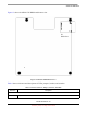
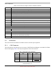
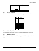
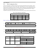
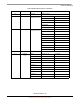
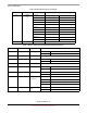
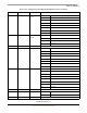
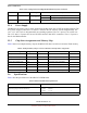
Table Of Contents
- About This Book
- 1 Introduction
- 2 MPC837xE-RDS Board
- 2.1 Board-Level Functions
- 2.1.1 Reset and Reset Configurations
- 2.1.2 External Interrupts
- 2.1.3 Clock Distribution
- 2.1.4 DDR2 SDRAM Controller
- 2.1.5 Local Bus Controller
- 2.1.6 Flash Memory
- 2.1.7 I2C
- 2.1.8 SATA Controller
- 2.1.9 PCI Express Interface (PCI-E & Mini PCI-E)
- 2.1.10 10/100/1000 BaseT Interface
- 2.1.11 RS-232 Port
- 2.1.12 USB 2.0 Interface
- 2.1.13 PCI Subsystem
- 2.1.14 COP/JTAG Port
- 2.2 MPC837xE-RDS Assembly
- 2.3 Connectors
- 2.4 LEDs
- 2.5 MPC837xE-RDS Board Configuration
- 2.6 Specifications
- 2.7 Mechanical Data
- 2.1 Board-Level Functions
- 3 Board Bootup
- 4 MPC837xE-RDS Software
- 5 Unit Assembly
- MPC837xE-RDS

MPC837xE-RDS, Rev. 1.0
30 Freescale Semiconductor
Preliminary, Subject to Change without Notice
MPC837xE-RDS Board
2.5.4 Power Supply
The MPC837xE requires a 48 V power supply from the DC power jack or PoE for normal operation. The
48 V power supply is reduced to 5 V and 3.3 V from the DC-DC circuitry on PoE daughter board. The
1.0 V, 1.5 V, and 1.8 V are all generated from switching regulators. The 1.0 V power is for a CPU core.
The 1.5 V and 1.8 V powers are for two GE PHYs and two mini PCI-E connectors. The 1.8 V power is
also for the DDR controller.
2.5.5 Chip-Select Assignments and Memory Map
Table 8 shows an example memory map on the MPC837xE that is used for u-boot in the Flash memory.
2.6 Specifications
Table 9 lists the specifications of the MPC837xE-RDS board.
.
30 LDP LDP/CKSTP pin
mux state after reset
0 LDP[0:3] = local data parity.
1: Default LDP[0:3] = LCS[4:7]
31 Reserved — Should be cleared
Table 8. Example Memory Map, Local Access Window, and Chip-Select Assignments
Address Range Target Interface Chip-Select Line Device Name Port Size (Bits)
0x0000_0000–0x1FFF_FFFF DDR MCS0 DDR2 SDRAM (512 Mbyte) 64
0x8000_0000–0x9FFF_FFFF PCI1 Nil PCI1 memory space (512 Mbyte) 32
0xE200_0000–0xE2FF_FFFF PCI1 Nil PCI1 I/O space (16 Mbyte) 32
0xA000_0000–0xBFFF_FFFF PCI2 Nil PCI2 memory space (512 Mbyte) 32
0xE300_0000–0xE3FF_FFFF PCI2 Nil PCI2 I/O space (16 Mbyte) 32
0xE000_0000–0xEFFF_FFFF Internal bus Nil IMMR (1 Mbyte) —
0xFC00_0000–0xFFFF_FFFF Local bus LCS0 NOR Flash memory (64 Mbyte) 16
Table 9. MPC837xE-RDS Board Specifications
Characteristics Specifications
Power requirements:
(Without any plugin card and USB device)
Typical
5.0 V DC 0.009 A
3.3 V DC 1.17 A
Communication processor MPC8377E running @ up to 667 MHz
Table 7. Reset Configuration Word High (RCWH) Bit Descriptions (continued)
Bits Name Meaning Detailed Description