
User's Guide
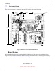
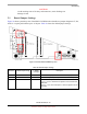
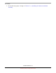
Table Of Contents
- About This Book
- 1 Introduction
- 2 MPC837xE-RDS Board
- 2.1 Board-Level Functions
- 2.1.1 Reset and Reset Configurations
- 2.1.2 External Interrupts
- 2.1.3 Clock Distribution
- 2.1.4 DDR2 SDRAM Controller
- 2.1.5 Local Bus Controller
- 2.1.6 Flash Memory
- 2.1.7 I2C
- 2.1.8 SATA Controller
- 2.1.9 PCI Express Interface (PCI-E & Mini PCI-E)
- 2.1.10 10/100/1000 BaseT Interface
- 2.1.11 RS-232 Port
- 2.1.12 USB 2.0 Interface
- 2.1.13 PCI Subsystem
- 2.1.14 COP/JTAG Port
- 2.2 MPC837xE-RDS Assembly
- 2.3 Connectors
- 2.4 LEDs
- 2.5 MPC837xE-RDS Board Configuration
- 2.6 Specifications
- 2.7 Mechanical Data
- 2.1 Board-Level Functions
- 3 Board Bootup
- 4 MPC837xE-RDS Software
- 5 Unit Assembly
- MPC837xE-RDS

MPC837xE-RDS, Rev. 1.0
32 Freescale Semiconductor
Preliminary, Subject to Change without Notice
Board Bootup
2.7 Mechanical Data
Figure 21 shows the MPC837xE-RDS dimensions (in mil). The board dimensions are 170 mm × 170 mm
(6693 mils × 6693 mils) for integration in a mini ITX chassis with a small footprint.
Figure 21. Dimensions of the MPC837xE-RDS Board
3 Board Bootup
This section describes how to boot up the MPC837xE-RDS board. The factory has preloaded a Flash
image onto the on-board Flash memory. Before powering up the board, set the on-board jumpers according
to the settings listed in Section 3.1, Board Jumper Settings.
6693.00
6693.00
2060.00
2590.00
1360.00
mounting hole
typ 4