
User's Guide
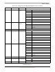
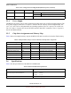
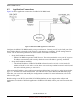
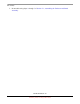
Table Of Contents
- About This Book
- 1 Introduction
- 2 MPC837xE-RDS Board
- 2.1 Board-Level Functions
- 2.1.1 Reset and Reset Configurations
- 2.1.2 External Interrupts
- 2.1.3 Clock Distribution
- 2.1.4 DDR2 SDRAM Controller
- 2.1.5 Local Bus Controller
- 2.1.6 Flash Memory
- 2.1.7 I2C
- 2.1.8 SATA Controller
- 2.1.9 PCI Express Interface (PCI-E & Mini PCI-E)
- 2.1.10 10/100/1000 BaseT Interface
- 2.1.11 RS-232 Port
- 2.1.12 USB 2.0 Interface
- 2.1.13 PCI Subsystem
- 2.1.14 COP/JTAG Port
- 2.2 MPC837xE-RDS Assembly
- 2.3 Connectors
- 2.4 LEDs
- 2.5 MPC837xE-RDS Board Configuration
- 2.6 Specifications
- 2.7 Mechanical Data
- 2.1 Board-Level Functions
- 3 Board Bootup
- 4 MPC837xE-RDS Software
- 5 Unit Assembly
- MPC837xE-RDS

Board Bootup
MPC837xE-RDS, Rev. 1.0
Freescale Semiconductor 33
Preliminary, Subject to Change without Notice
CAUTION
Avoid touching areas of circuitry and connectors; static discharge can
damage circuits.
3.1 Board Jumper Settings
Figure 22 shows a partial top view of the MPC837xE-RDS with red outlines at jumper designators J7, J10,
and J12. A square pad indicates pin 1 of the part. Table 10 shows the default jumper settings.
Figure 22. Partial MPC837xE-RDS Top View
Table 10. Default Jumper Settings
Reference Default Jumper Setting
√ = Jumper
× = No Jumper
Description
J7 × Watchdog input for MAX6829. Default is no jumper.
J10 × 12V external power input for optional connector---X1 PCI Express.
J12 2–3 √ Select the reset configuration source (RST-CFG-SRC) for the MPC837xE.
Jumper 2-3 (default): 0000 Reset configuration word is loaded from
NOR Flash.
Jumper 1-2: 1111 Hard-coded option 7. Reset configuration word is
not loaded.