
User's Guide
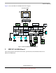
Table Of Contents
- About This Book
- 1 Introduction
- 2 MPC837xE-RDS Board
- 2.1 Board-Level Functions
- 2.1.1 Reset and Reset Configurations
- 2.1.2 External Interrupts
- 2.1.3 Clock Distribution
- 2.1.4 DDR2 SDRAM Controller
- 2.1.5 Local Bus Controller
- 2.1.6 Flash Memory
- 2.1.7 I2C
- 2.1.8 SATA Controller
- 2.1.9 PCI Express Interface (PCI-E & Mini PCI-E)
- 2.1.10 10/100/1000 BaseT Interface
- 2.1.11 RS-232 Port
- 2.1.12 USB 2.0 Interface
- 2.1.13 PCI Subsystem
- 2.1.14 COP/JTAG Port
- 2.2 MPC837xE-RDS Assembly
- 2.3 Connectors
- 2.4 LEDs
- 2.5 MPC837xE-RDS Board Configuration
- 2.6 Specifications
- 2.7 Mechanical Data
- 2.1 Board-Level Functions
- 3 Board Bootup
- 4 MPC837xE-RDS Software
- 5 Unit Assembly
- MPC837xE-RDS

MPC837xE-RDS, Rev. 1.0
8 Freescale Semiconductor
Preliminary, Subject to Change without Notice
Introduction
– Two standard External SATA connectors
— PCI: 32-bit PCI interface up to 66 Mhz
– 2x 32-bit 3.3 V mini PCI slots
— PCI Express
– Two mini PCI Express Connectors, or
– One mini PCI Express connector and one PCI Express x1 connector
—SDHC
– One SDHC Card Connector
—I
2
C
–I
2
C connected to ST M24256 Serial EEPROM
— Board Connectors
– One DC power jack
– One internal 2 x 5 RS-232 connector
– JTAG / COP for debugging
— Form factor
– Mini ITX form factor (170 mm x 170 mm, or 6693 mils x 6693 mils)
• 6-layer PCB (4 layers signals and separate power and ground layers)
• Certification
—CE/FCC
• Lead-Free (RoHS)