
DSP Core Reference Manual

5-34 SC140 DSP Core Reference Manual
Stack Support
5.5.3 Stack Support Instructions
The core provides push and pop instructions that reference the active stack pointer (NSP or ESP).
Table 5-11 describes these instructions.
In addition, the stack can be accessed with move or bit mask instructions that use short and word
displacement addressing with the stack pointer as a base pointer. However, these instructions do not
change the value of the stack pointer. Generally, the stack pointer points to the next unoccupied location.
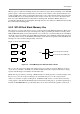
While using the pop/push instructions, all SC140 registers are viewed as two separate banks, an even
register file bank and an odd register file bank (as shown in Table 5-12).
Up to two push instructions are supported in a single execution set. If two push instructions are included in
a single execution set, one push instruction must use an even register operand, and the other push
instruction must use an odd register operand. A push instruction always pushes one 32-bit register into the
stack. Any execution set that includes one or two push instructions increments the stack pointer by eight. In
the case of a single push, a single operand is written to the memory while the adjacent memory location
remains unchanged.
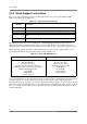
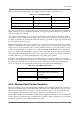
Table 5-11. Stack Push/Pop Instructions
Instruction Description
POP Pre-decrement the stack by eight and restore one 32-bit register
POPN Same as POP, but using the NSP regardless of the working mode
PUSH Push a single 32-bit register onto the active stack and increment the pointer by
eight
PUSHN Same as PUSH, but using the NSP regardless of the working mode
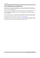
Table 5-12. Even and Odd Registers
Even Register (De) File Odd Register (Do) File
D0 D2 D4 D6 D8 D10 D12 D14
D0.e D2.e D4.e D6.e
D8.e D10.e D12.e D14.e
D0.e:D1.e D2.e:D3.e D4.e:D5.e D6.e:D7.e
D8.e:D9.e D10.e:D11.e D12.e:D13.e D14.e:D15.e
R0 R2 R4 R6 R8 R10 R12 R14
B0 B2 B4 B6
N0 N2 M0 M2
SA0 SA1 SA2 SA3
D1 D3 D5 D7 D9 D11 D13 D15
D1.e D3.e D5.e D7.e
D9.e D11.e D13.e D15.e
R1 R3 R5 R7 R9 R11 R13 R15
B1 B3 B5 B7
N1 N3 M1 M3
LC0 LC1 LC2 LC3
VBA SR MCTL