
Reference Manual
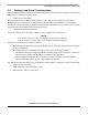


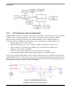


Table Of Contents

USB-KW24D512
USB-KW2x Hardware Reference Manual, Rev. 0.1
3-4 Freescale Semiconductor
Figure 3-3. USB-KW24D512 Block Diagram
3.2.1 RF Performance and Considerations
USB-KW24D512 transceiver includes a 1mW nominal output power, PA with internal voltage controlled
oscillator (VCO), integrated transmit/receive switch, on-board power supply regulation, and full
spread-spectrum encoding and decoding. The USB-KW24D512 utilizes a minimum number of
components while providing good RF performance. Key specifications for USB-KW24D512 are:
• Nominal output power is set to 0 dBm
• Programmable output power from –32 dBm to +8 dBm measured at the antenna feed
• Typical sensitivity is -101 dBm (@1% PER for 25 °C) measured at the antenna feed
• Frequency range is 2360 to 2480 MHz
• Folded “F” printed metal antenna for a small footprint, low cost design
• Uses a minimum number of RF marching components and external 50:50 balun
An external 50 (unbal): 50(bal) balun connects a single-ended 50-ohm port to the differential RF port of
the MKW24D512 radio. The layout has provision for out-of-band signal suppression (components L5 and
C19) if required. Figure 3-4 shows the typical topology for the RF circuitry. The RF switch J4 has been
designed in for measurement purposes and is left as DNP.
Figure 3-4. USB-KW24D512 RF Circuitry