
User Manual
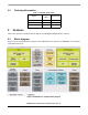

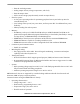

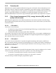


Table Of Contents
- 1 Introduction
- 2 Features
- 3 Transceiver description
- 4 System and power management
- 5 Radio Peripherals
- 6 MKW2xDxxxV operating modes
- 7 MKW2xDxxxV electrical characteristics
- 8 MCU Electrical characteristics
- 8.1 Maximum ratings
- 8.2 General
- 8.3 LVD and POR operating requirements
- 8.4 Switching specification
- 8.5 Core modules
- 8.6 Clock modules
- 8.7 Memories and memory interfaces
- 8.8 Analog
- 8.9 Communication interfaces
- 8.9.1 USB electrical specifications
- 8.9.2 USB DCD electrical specifications
- 8.9.3 VREG electrical specifications
- 8.9.4 DSPI switching specifications (limited voltate range)
- 8.9.5 DSPI switching specification (full voltage range)
- 8.9.6 Normal Run, Wait and Stop mode performance over the fulloperating voltage range
- 8.9.7 VLPR, VLPW, and VLPS mode performance over the full operating voltage range
- 9 Transceiver electrical characteristics
- 10 Crystal oscillator reference frequency
- 11 Pin assignments
- 12 Packaging information

MKW2xDxxxV Product Electrical Specification, Rev. 0.1
2 Freescale Semiconductor
1.1 Ordering information
2Features
This section provides a simplified block diagram and highlights MKW2xDxxxV features.
2.1 Block diagram
Figure 1 shows a simplified block diagram of the MKW2xDxxxV, which is an IEEE®802.15.4 standard
compatible transceiver.
Figure 1. MKW2xDxxxV simplified block diagram
Table 1. Orderable parts details
Device
Program
flash
System RAM
MKW24D512V (USB) 512 K 64 K
MKW22D512V (USB) 512 K 64 K
MKW21D256V 256 K 32 K