
User Manual
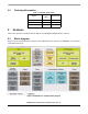


Table Of Contents
- 1 Introduction
- 2 Features
- 3 Transceiver description
- 4 System and power management
- 5 Radio Peripherals
- 6 MKW2xDxxxV operating modes
- 7 MKW2xDxxxV electrical characteristics
- 8 MCU Electrical characteristics
- 8.1 Maximum ratings
- 8.2 General
- 8.3 LVD and POR operating requirements
- 8.4 Switching specification
- 8.5 Core modules
- 8.6 Clock modules
- 8.7 Memories and memory interfaces
- 8.8 Analog
- 8.9 Communication interfaces
- 8.9.1 USB electrical specifications
- 8.9.2 USB DCD electrical specifications
- 8.9.3 VREG electrical specifications
- 8.9.4 DSPI switching specifications (limited voltate range)
- 8.9.5 DSPI switching specification (full voltage range)
- 8.9.6 Normal Run, Wait and Stop mode performance over the fulloperating voltage range
- 8.9.7 VLPR, VLPW, and VLPS mode performance over the full operating voltage range
- 9 Transceiver electrical characteristics
- 10 Crystal oscillator reference frequency
- 11 Pin assignments
- 12 Packaging information

MKW2xDxxxV Product Electrical Specification, Rev. 0.1
Freescale Semiconductor 3
2.2 Radio features
• 2.4 GHz frequency band of operation
• 250 kbps data rate with O-QPSK modulation in 5.0 MHz channels with direct sequence
spread-spectrum (DSSS) encode and decode
• Operates on one of 16 selectable channels per IEEE 802.15.4 specification
• Programmable output power
• Supports 2.36 to 2.4 GHz Medical Band (MBAN) frequencies with same modulation as IEEE
802.15.4
• Small RF footprint
— Differential input/output port used with external balun
— Integrated transmit/receive switch
— Supports single ended and diversity antenna options
— Low external component count
— Supports external PA and LNA
• Hardware acceleration for IEEE® 802.15.4 2006 packet processing
— Random number generator
— Support for dual PAN mode
• 32 MHz crystal reference oscillator with on board trim capability to supplement external load
capacitors
• Programmable frequency clock output (CLK_OUT)
• Bit stream mode (BSM) to monitor packet data with synchronization clock
• Advanced Security Module with support for AES encryption
• GPIO for Antenna Diversity control
•Clocks
— 32 MHz crystal oscillator
— Internal 1 kHz low power oscillator
— DC to 32 MHz external square wave input clock
2.3 Microcontroller features
In addition all MKW2xDxxxV devices contain the below microcontroller features:
•Core:
— ARM Cortex-M4 Core delivering 1.25 DMIPS/MHz with DSP instructions (floating-point unit
available on certain Kinetis families)
— 16-channel DMA for peripheral and memory servicing with minimal CPU intervention
• Reliability, Safety and Security:
— Hardware cyclic redundancy check engine for validating memory contents/communication
data and increased system reliability
— Independent-clocked COP for protection against code runaway in fail-safe applications