
User Manual
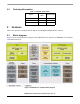


Table Of Contents
- 1 Introduction
- 2 Features
- 3 Transceiver description
- 4 System and power management
- 5 Radio Peripherals
- 6 MKW2xDxxxV operating modes
- 7 MKW2xDxxxV electrical characteristics
- 8 MCU Electrical characteristics
- 8.1 Maximum ratings
- 8.2 General
- 8.3 LVD and POR operating requirements
- 8.4 Switching specification
- 8.5 Core modules
- 8.6 Clock modules
- 8.7 Memories and memory interfaces
- 8.8 Analog
- 8.9 Communication interfaces
- 8.9.1 USB electrical specifications
- 8.9.2 USB DCD electrical specifications
- 8.9.3 VREG electrical specifications
- 8.9.4 DSPI switching specifications (limited voltate range)
- 8.9.5 DSPI switching specification (full voltage range)
- 8.9.6 Normal Run, Wait and Stop mode performance over the fulloperating voltage range
- 8.9.7 VLPR, VLPW, and VLPS mode performance over the full operating voltage range
- 9 Transceiver electrical characteristics
- 10 Crystal oscillator reference frequency
- 11 Pin assignments
- 12 Packaging information

MKW2xDxxxV Product Electrical Specification, Rev. 0.1
Freescale Semiconductor 7
— Data rate: 250 kbps
— Symbol rate: 62.5 kbps
— Modulation: OQPSK
• Receiver sensitivity: –102 dBm, typical (@1% PER for 20 byte payload packet)
• Differential bidirectional RF input/output port with integrated transmit/receive switch
• Programmable output power from –30 dBm to +10 dBm.
3.2 RF interface and usage
The MKW2xDxxxV RF output ports are bidirectional (diplexed between receive/transmit modes) and
differential enabling interfaces with numerous off-chip devices such as a balun. When using a balun, this
device provides an interface to directly connect between a single-ended antenna with MKW2xDxxxV RF
ports. In addition, MKW2xDxxxV provides four output driver ports that can have both drive strength and
slew rate configured to control external peripheral devices. These signals designated ANT_A, ANT_B,
RX_SWITCH, and TX_SWITCH when enabled are switched via an internal hardware state machine.
These ports provide control features for peripheral devices such as:
• Antenna diversity modules
• External PAs
• External LNAs
• T/R switched
3.2.1 Clock output feature
The CLK_OUT digital output can be enabled to drive the system clock to the MCU. This provides a highly
accurate clock source based on the transceiver reference oscillator. The clock is programmable over a wide
range of frequencies divided down from the reference 32 MHz (see Table 3).The CLK_OUT pin will be
enabled upon POR. The frequency CLK_OUT will be determined by the state of the GPIO5/BOPT pin. If
this pin is low upon POR, then the frequency will be 4 MHz (32 MHz/8). If this pin is high upon POR
(upon POR GPIO5 has a pullup resistor) then the frequency will be 32.78689 kHz (32 MHz/976).
3.3 Transceiver functions
3.3.1 Receive path
The receive path has the functionality to operate in run state or operate in a low power run state (LPRS)
that can be considered as a partial power down mode. The radio receiver path is based upon a near zero IF
(NZIF) architecture incorporating front end amplification, one(1) mixed signal down conversion to IF that
is programmably filtered, demodulated and digitally processed. The RF front end (FE) input port is
differential that shares the same off chip matching network with the transmit path.