
Datasheet


MPX4250A
Sensors
6 Freescale Semiconductor
Pressure
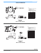
INFORMATION FOR USING THE SMALL OUTLINE PACKAGE (CASE 482)
MINIMUM RECOMMENDED FOOTPRINT FOR SURFACE MOUNTED APPLICATIONS
Surface mount board layout is a critical portion of the total
design. The footprint for the surface mount packages must be
the correct size to ensure proper solder connection interface
between the board and the package. With the correct
Footprint, the packages will self align when subjected to a
solder reflow process. It is always recommended to design
boards with a solder mask layer to avoid bridging and
shorting between solder pads.
Figure 5. SOP Footprint (Case 482)
0.660
16.76
0.060 TYP 8X
1.52
0.100 TYP 8X
2.54
0.100 TYP 8X
2.54
0.300
7.62
inch
mm
SCALE 2:1