
Datasheet


Electrical Specifications
44 Quad-Core Intel® Xeon® Processor 5300 Series Datasheet
Note:
1. Unless otherwise noted, all specifications in this table apply to all processor frequencies.
2. The tolerances for this specification have been stated generically to enable system designer to calculate the
minimum values across the range of V
TT
.
3. GTLREF_DATA_MID, GTLREF_DATA_END, GTLREF_ADD_MID, and GTLREF_ADD_END is generated from V
TT
on the baseboard by a voltage divider of 1% resistors. The minimum and maximum specifications account
for this resistor tolerance. Refer to the appropriate platform design guidelines for implementation details.
The V
TT
referred to in these specifications is the instantaneous V
TT
.
4. R
TT
is the on-die termination resistance measured at V
OL
of the AGTL+ output driver. Measured at
0.31*V
TT
. R
TT
is connected to V
TT
on die. Refer to processor I/O Buffer Models for I/V characteristics.
5. COMP resistance must be provided on the system board with +/- 1% resistors. See the applicable platform
design guide for implementation details.
Note:
1. Unless otherwise noted, all specifications in this table apply to all processor frequencies.
2. Rise and fall times are measured single-ended between 245 mV and 455 mV of the clock swing.
3. Crossing Voltage is defined as the instantaneous voltage value when the rising edge of BCLK0 is equal to
the falling edge of BCLK1.
4. V
Havg
is the statistical average of the V
H
measured by the oscilloscope.
5. Overshoot is defined as the absolute value of the maximum voltage.
6. Undershoot is defined as the absolute value of the minimum voltage.
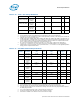
Table 2-20. AGTL+ Bus Voltage Definitions
Symbol Parameter Min Typ Max Unit Notes
1
GTLREF_DATA_MID
GTLREF_DATA_END
Data Bus
Reference
Voltage
0.98 * 0.67 * V
TT
0.67 * V
TT
1.02 * 0.67 * V
TT
V2, 3
GTLREF_ADD_MID
GTLREF_ADD_END
Address Bus
Reference
Voltage
0.98 * 0.67 * V
TT
0.67 * V
TT
1.02 * 0.67 * V
TT
V2, 3
R
TT
Termination
Resistance
(pull up)
45 50 55 Ω 4
COMP COMP
Resistance
49.4 49.9 50.4 Ω 5
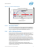
Table 2-21. FSB Differential BCLK Specifications
Symbol Parameter Min Typ Max Unit Figure
Notes
1,2
V
L
Input Low
Voltage
-0.150 0.0 N/A V 2-15
V
H
Input High
Voltage
0.660 0.710 0.850 V 2-15
V
CROSS(abs)
Absolute
Crossing
Point
0.250 0.350 0.550 V 2-15,
2-16
3,9
V
CROSS(rel)
Relative
Crossing
Point
0.250 +
0.5 * (V
Havg
- 0.700)
N/A 0.550 +
0.5 * (V
Havg
- 0.700)
V 2-15,
2-16
4,9,10
Δ V
CROSS Range of
Crossing
Points
N/A N/A 0.140 V 2-15,
2-16
12
V
OS
Overshoot N/A N/A VH + 0.300 V 2-15 5
V
US
Undershoot -0.300 N/A N/A V 2-15 6
V
RBM
Ringback
Margin
0.200 N/A N/A V 2-15 7
V
TR
Threshold
Region
V
CROSS
- 0.100 N/A V
CROSS
+ 0.100 V 2-15 8
I
LI
Input
Leakage
Current
N/A N/A +/- 100 μA11