FUJITSU MICROELECTRONICS DATA SHEET DS04–21348–3Ea ASSP Single Serial Input PLL Frequency Synthesizer On-Chip prescaler MB15C02 ■ DESCRIPTION The Fujitsu Microelectronics MB15C02 is a serial input Phase Locked Loop (PLL) frequency synthesizer with a prescaler. A 64/65 division is available for the prescaler that enables pulse swallow operation. This operates with a supply voltage of 1.0 V (min.). MB15C02 is suitable for mobile communications, such as paging systems.
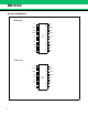
MB15C02 ■ PIN ASSIGNMENTS SSOP-20 pin VDD 1 20 VSS Clock 2 19 OSCIN NC 3 18 NC Data 4 17 OSCOUT LE 5 Top View 16 fin 6 15 FC PS 7 14 φP NC 8 13 NC LD 9 12 φR Do 10 11 Vp TEST (FPT-20P-M03) SSOP-16 pin VDD 1 16 VSS Clock 2 15 OSCIN Data 3 14 OSCOUT LE 4 13 TEST fin 5 12 FC PS 6 11 φP LD 7 10 φR Do 8 9 Vp Top View (FPT-16P-M05) 2
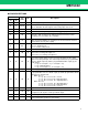
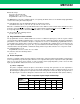
MB15C02 ■ PIN DESCRIPTIONS Pin no. SSOP SSOP 16 20 Pin name I/O Descriptions 1 1 VDD – Power supply voltage 2 2 Clock I Clock input for the shift register.(Schmitt trigger input) Data is shifted into the shift register on the rising edge of the clock. – 3 NC – No connection 3 4 Data I Serial data input using binary code.
MB15C02 (Continued) Pin no. SSOP SSOP 16 20 4 Pin name I/O Descriptions 14 17 OSCOUT O Oscillator output. Connection for an external crystal. – 18 NC – No connection 15 19 OSCIN I Programmable reference divider input. Oscillator input. Clock can be input to OSCIN from outside. In the case, please leave OSCOUT pin open and make connection with OSCIN as AC coupling. 16 20 VSS – Ground pin.
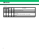
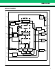
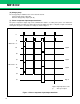
MB15C02 ■ BLOCK DIAGRAM Crystal oscillator circuit VDD Programmable reference divider VSS OSCIN Binary 14-bit reference counter Intermittent mode control circuit 14 OSCOUT 14-bit latch Clock fr Phase comparator fp 14 18-bit shift register Data TEST Control register FC Output control circuit φP Output control circuit φR 18 LE 18-bit latch 6 12 fin PS Prescaler Binary 6-bit swallow counter Binary 12-bit programmable counter Charge pump VP LD Lock detector Control circuit Do 5
MB15C02 ■ ABSOLUTE MAXIMUM RATINGS Parameter Symbol Power supply voltage Rating Unit Min. Max. VDD, VP GND–0.5 +2.0 V VIN GND–0.5 VDD +0.5 V Output voltage VOUT GND–0.5 VDD +0.5 V Output current IOUT –10 +10 mA Storage temperature Tstg –40 +125 °C Input voltage Remark WARNING: Semiconductor devices can be permanently damaged by application of stress (voltage, current, temperature, etc.) in excess of absolute maximum ratings. Do not exceed these ratings.
MB15C02 ■ ELECTRICAL CHARACTERISTICS (For 220 MHz :VDD = Vp = 1.0 to 1.5 V, Ta = –20 to +60°C) (For 330 MHz :VDD = Vp = 1.2 to 1.5 V, Ta = –20 to +60°C) (For 450 MHz :VDD = Vp = 1.3 to 1.5 V, Ta = –20 to +60°C) Parameter Symbol Condition Value Min. Typ.*3 Max.*4 Unit Power supply current Active Mode IDD *1 (VDD=1.0V/220MHz) (VDD=1.2V/330MHz) (VDD=1.3V/450MHz) – – – 0.6 1.0 1.3 1.2 1.8 2.2 mA Power saving current Power saving mode IDDS *2 (VDD=1.0V) (VDD=1.2V) (VDD=1.
MB15C02 ■ FUNCTION DESCRIPTIONS 1.
MB15C02 Divide ratio range: Prescaler : M = 64, M+1=65 Swallow counter : A = 0 to 63 Programmable counter : N = 5 to 4095 The MB15C02 uses the pulse swallow method; consequently, the divide rations of the swallow and programmable counters must satisfy the relationship N>A.
MB15C02 (b) Charge pump The charge pump is available in two forms: internal external. Internal charge pump output (Do) External charge pump outputs (φR, φP) (c) Phase comparator input/output waveforms The phase comparator outputs logic levels summarized in Table 1, according to the phase error between fr and fp. Note that φP is an Nch open drain output. The pulse width of the phase comparator outputs are identical and equal to the phase error between fr and fp as shown in Figure 1.
MB15C02 (d) Lock detector The lock detector detects the lock and unlock states of the PLL. The lock detector outputs “H” when the PLL enters the lock state and outputs “L” when the PLL enters the unlock state as shown in Figure 2. When PS = “L”, the lock detector outputs “H” compulsorily. fr fp LD Figure 2.
MB15C02 4. Setting the Divide Ratio (1) Serial data format The format of the serial data is shown is Figure 3. The serial data is composed of a control bit and divide ratio setting data. The control bit selects the programmable divider or programmable reference divider. In case of the programmable divider, serial data consists of 18 bits(6 bits for the swallow counter and 12 bits for the programmable counter) and 1 control bit as shown in Figure 3.1.
MB15C02 (2) The flow of serial data Serial data is received via data pin in synchronization with the clock input and loaded into shift register which contains the divide ratio setting data and into the control register which contains the control bit. The logical product (through the AND gate in Figure 4) of LE and the control register output (i.e., control bit) is fed to the enable input of the latches.
MB15C02 (4) Setting the divide ratio for the programmable reference divider Columns R0-R13 of Table 3 represent the divide ratio of the programmable reference counter. The control bit is set to 1. Table.
MB15C02 Since the divide rations are unpredictable when the MB15C02 is turned on, it is necessary to initialize the divide ratio for both dividers at power-on time. As shown in Figure 6, after setting the divide ratio for one of the dividers (e.g., programmable reference divider), set LE to “H” level before setting the divide ratio for the other dividers (e.g., programmable divider).
MB15C02 ■ TYPICAL CHARACTERISTICS 1. fin Input Sensitivity fin input frequency vs. Input sensitivity 20.0 Ta = +25°C 10.0 Input sensitivity (dBm) 0.0 −10.0 −20.0 −30.0 −40.0 V DD = 1.0 V V DD = 1.2 V V DD = 1.3 V V DD = 1.5 V −50.0 −60.0 0 100 200 300 400 500 600 700 800 900 1000 fin input frequency (MHz) 2. OSCIN Input Sensitivity OSC IN input frequency vs. Input sensitivity 20.0 Ta = +25°C 10.0 Input sensitivity (dBm) 0.0 −10.0 −20.0 −30.0 −40.0 V DD = 1.0 V V DD = 1.2 V V DD = 1.
MB15C02 3. fin Power Supply Voltage Power supply voltage vs. fin input frequency (MHz) 1000 900 Ta = +25°C Vfin = −2.0 (dBm) Input frequency (MHz) 800 700 600 500 400 300 200 100 0 0.9 1.0 1.1 1.2 1.3 1.4 1.5 1.6 1.7 1.8 Power supply voltage (V) 4. OSCIN Power Supply Voltage Power supply voltage vs. OSC IN input frequency 500 450 Ta = +25°C Vfin = −2.0 (dBm) 400 Input frequency (MHz) 350 300 250 200 150 100 50 0 0.9 1.0 1.1 1.2 1.3 1.4 1.5 1.6 1.7 1.
MB15C02 5. IDD Power Supply Current Input frequency vs. power supply current 5.0 Ta = +25°C 4.5 4.0 I DD (mA) 3.5 3.0 2.5 2.0 1.5 V DD = 1.0 V V DD = 1.2 V V DD = 1.3 V V DD = 1.5 V 1.0 0.5 0.
MB15C02 6. Do (Charge Pump) Power Supply Voltage V DD (V p) vs. I OL (at V OL = 0.2 V) 5.0 Ta = +25°C 4.5 4.0 I OL (mA) 3.5 3.0 2.5 2.0 1.5 1.0 0.5 0.0 0.8 0.9 1.0 1.1 1.2 1.3 1.4 1.5 1.6 1.7 1.8 V DD (V) V DD (V p) vs. I OH (at V OH = V DD – 0.2 V) –5.0 Ta = +25°C –4.5 –4.0 –3.5 I OH (mA) –3.0 –2.5 –2.0 –1.5 –1.0 –0.5 0.0 0.8 0.9 1.0 1.1 1.2 1.3 1.4 1.5 1.6 1.7 1.
MB15C02 7. Spectrum Wave Form ATTEN 10 dB RL 0 dBm ∆MKR −85.50 dB 25.0 kHz UAUG 16 10dB/ • LOCK Frequency : 286.0 MHz (fr = 25 kHz) • V DD = 1.2 V, V p = 1.2 V Ta = +25°C ∆MKR D 25.0 kHz S −85.50 dB CENTER 286.0000 MHz *RBW 1.0 kHz VBW 1.0 kHz ATTEN 10 dB RL 0 dBm SPAN 200.0 kHz *SWP 1.00 s ∆MKR −53.84 dB 800 Hz UAUG 50 10dB/ • LOCK Frequency : 286.0 MHz ( fr = 25 kHz) • VDD = 1.2 V, V p = 1.2 V Ta = +25°C ∆MKR D 800 Hz S −53.84 dB CENTER 286.00000 MHz *RBW 100 Hz VBW 100 kHz SPAN 20.
MB15C02 8. Lock Up Time • LOCK Frequency: 290.0 MHz to 286.0 MHz (fr = 25 kHz) • VDD = 1.2 V, VP = 1.2 V, Ta = +25°C 290.0 MHz → 286.0 MHz, within ± 1 kHz 4.00 ms ∆MKr x : 3.99999984 ms y : −4.00100 MHz A euts N/A 286.0050 MHz 2.00 kHz/div 285.9950 MHz 0 s 10.0000000 ms • LOCK Frequency: 286.0 MHz to 290.0 MHz (fr = 25 kHz) • VDD = 1.2 V, VP = 1.2 V, Ta = +25°C 286.0 MHz → 290.0 MHz, within ± 1 kHz 6.20 ms ∆MKr x : 6.19999943 ms y : 4.00082 MHz A euts N/A 290.0050 MHz 2.00 kHz/div 289.
MB15C02 (Continued) • LOCK Frequency: PS on to 286.0 MHz (fr = 25 kHz) • VDD = 1.2 V, VP = 1.2 V, Ta = +25°C PS ON → 286.0 MHz, within ± 1 kHz 2.00 ms ∆MKr x : 1.99999978 ms y : −680 Hz A euts N/A 286.0050 MHz 2.00 kHz/div 285.9950 MHz 0 s PS 8.0000000 ms 1V 0V ■ USAGE PRECAUTIONS • This device should be transported and stored in anti-static containers. • This is a static-sensitive device; take proper anti-ESD precautions. Ensure that personnel and equipment are properly grounded.
MB15C02 ■ PACKAGE DIMENSIONS 16 pins, Plastic SSOP (FPT-16P-M05) *: These dimensions do not include resin protrusion. +0.20 * 5.00±0.10(.197±.004) 1.25 –0.10 +.008 .049 –.004 (Mounting height) 0.10(.004) INDEX *4.40±0.10 (.173±.004) 0.65±0.12 (.0256±.0047) 4.55(.179)REF C 1994 FUJITSU LIMITED F16013S-2C-4 +0.10 0.22 –0.05 +.004 .009 –.002 6.40±0.20 (.252±.008) 5.40(.213) NOM "A" +0.05 0.15 –0.02 +.002 .006 –.001 Details of "A" part 0.10±0.10(.004±.004) (STAND OFF) 0 10° 0.50±0.20 (.
MB15C02 (Continued) 20 pins, Plastic SSOP (FPT-20P-M03) *: These dimensions do not include resin protrusion. +0.20 * 6.50±0.10(.256±.004) 1.25 –0.10 +.008 .049 –.004 (Mounting height) 0.10(.004) INDEX *4.40±0.10 6.40±0.20 (.173±.004) (.252±.008) 0.65±0.12 (.0256±.0047) 5.85(.230)REF C 24 1994 FUJITSU LIMITED F20012S-2C-4 +0.10 0.22 –0.05 +.004 .009 –.002 "A" 5.40(.213) NOM +0.05 0.15 –0.02 +.002 .006 –.001 Details of "A" part 0.10±0.10(.004±.004) (STAND OFF) 0 10° 0.50±0.20 (.020±.
MB15C02 MEMO 25
MB15C02 MEMO 26
MB15C02 MEMO 27
FUJITSU MICROELECTRONICS LIMITED Shinjuku Dai-Ichi Seimei Bldg. 7-1, Nishishinjuku 2-chome, Shinjuku-ku, Tokyo 163-0722, Japan Tel: +81-3-5322-3347 Fax: +81-3-5322-3387 http://jp.fujitsu.com/fml/en/ For further information please contact: North and South America FUJITSU MICROELECTRONICS AMERICA, INC. 1250 E. Arques Avenue, M/S 333 Sunnyvale, CA 94085-5401, U.S.A. Tel: +1-408-737-5600 Fax: +1-408-737-5999 http://www.fma.fujitsu.com/ Asia Pacific FUJITSU MICROELECTRONICS ASIA PTE LTD.