FUJITSU SEMICONDUCTOR DATA SHEET DS04-27231-3E ASSP For Power Management Applications (General Purpose DC/DC Converter) 2-ch DC/DC Converter IC with Overcurrent Protection MB39A104 ■ DESCRIPTION The MB39A104 is a 2-channel DC/DC converter IC using pulse width modulation (PWM), incorporating an overcurrent protection circuit (requiring no current sense resistor). This IC is ideal for down conversion. Operating at high frequency reduces the value of coil.
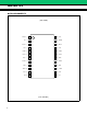
MB39A104 ■ PIN ASSIGNMENTS (TOP VIEW) VCCO : 1 24 : CTL VH : 2 23 : GNDO OUT1 : 3 22 : OUT2 VS1 : 4 21 : VS2 ILIM1 : 5 20 : ILIM2 DTC1 : 6 19 : DTC2 VCC : 7 18 : GND CSCP : 8 17 : VREF FB1 : 9 16 : FB2 −INE1 : 10 15 : −INE2 CS1 : 11 14 : CS2 RT : 12 13 : CT (FPT-24P-M03) 2
MB39A104 ■ PIN DESCRIPTION Pin No. Symbol I/O Descriptions 1 VCCO Output circuit power supply terminal (Connect to same potential as VCC pin.) 2 VH O Power supply terminal for FET drive circuit (VH = VCC − 5 V) 3 OUT1 O External Pch MOS FET gate drive terminal 4 VS1 I Overcurrent protection circuit input terminal 5 ILIM1 I Overcurrent protection circuit detection resistor connection terminal.
MB39A104 ■ BLOCK DIAGRAM −INE1 10 VREF 10 µA CS1 11 PWM + Comp.1 + − 1.24 V 1 VCCO CH1 L priority Error − Amp1 + + Drive1 Pch 3 OUT1 L priority FB1 9 IO = 200 mA at VCCO = 12 V Current Protection Logic − 4 VS1 + 5 ILIM1 DTC1 6 −INE2 15 VREF 10 µA CS2 14 1.24 V CH2 L priority Error − Amp2 + + PWM + Comp.2 + − Drive2 Pch FB2 16 IO = 200 mA at VCCO = 12 V DTC2 19 Current Protection Logic H priority H: at SCP SCP Comp. + + − (3.
MB39A104 ■ ABSOLUTE MAXIMUM RATINGS Parameter Symbol Power supply voltage VCC Output current Condition Rating Unit Min Max VCC, VCCO terminal 20 V IO OUT1, OUT2 terminal 60 mA Output peak current IOP Duty ≤ 5% (t = 1/fOSC×Duty) 700 mA Power dissipation PD Ta ≤ +25 °C 740* mW −55 +125 °C Storage temperature TSTG * : The packages are mounted on the epoxy board (10 cm × 10 cm).
MB39A104 ■ ELECTRICAL CHARACTERISTICS (VCC = VCCO = 12 V, VREF = 0 mA, Ta = +25 °C) 7.Error amplifier 6.Soft2.Under 5.Triangular 4.Short-circuit 3.Short-circuit bolck start voltage lockout wave oscillator detection block detection block [Error Amp1, block protection circuit block [OSC] [SCP Comp] [SCP Logic] Error Amp2] [CS1, CS2] block [UVLO] 1.
MB39A104 (Continued) (VCC = VCCO = 12 V, VREF = 0 mA, Ta = +25 °C) 13.Control block 14.General [CTL] 12.Output block [Drive1, Drive2] 11.Bias 10.Overcurrent 9.PWM comparator 8.Error amplifier bolck voltage protection circuit block [Error Amp1, block block [PWM Comp.1, Error Amp2] [VH] [OCP1, OCP2] PWM Comp.2] Parameter Symbol Pin No. BW 9, 16 VOH 9, 16 VOL 9, 16 ISOURCE 9, 16 ISINK Conditions Value Unit Min Typ Max 1.6* MHz 4.7 4.
MB39A104 ■ TYPICAL CHARACTERISTICS Power Supply Current vs. Power Supply Voltage 10 Reference voltage VREF (V) Ta = +25 °C CTL = 5 V 8 6 4 2 Ta = +25 °C CTL = 5 V VREF = 0 mA 8 6 4 2 0 0 0 5 10 15 20 0 5 10 15 20 Power supply voltage VCC (V) Power supply voltage VCC (V) Reference Voltage vs. Ambient Temperature Reference Voltage vs. Ambient Temperature Reference voltage VREF (V) 10 2.
MB39A104 Triangular Wave Oscillation Frequency vs. Timing Capacitor 10000 Ta = +25 °C VCC = 12 V CTL = 5 V 1000 CT = 39 pF CT = 560 pF 100 CT = 220 pF CT = 100 pF 10000 Triangular wave oscillattion frequency fOSC (kHz) Triangular wave oscillation frequency fOSC (kHz) Triangular Wave Oscillation Frequency vs. Timing Resistor Ta = +25 °C VCC = 12 V CTL = 5 V 1000 RT = 11 kΩ 100 RT = 130 kΩ 10 10 1 10 100 10 1000 100 Timing resistor RT (kΩ) 3.
MB39A104 (Continued) Error Amplifier, Gain, Phase vs. Frequency Ta = +25 °C VCC = 12 V 180 40 ϕ 90 Phase φ (deg) 20 Gain AV (dB) 240 kΩ AV 30 10 0 0 −10 −20 −90 −30 −180 100 1k 10 k 100 k 1M 10 M Frequency f (Hz) Power Dissipation vs. Ambient Temperature Power dissipation PD (mW) 1000 10 + IN 10 kΩ 2.4 kΩ (15) 10 − 11 (14) + + 1.
MB39A104 ■ FUNCTIONS 1. DC/DC Converter Functions (1) Reference voltage block (REF) The reference voltage circuit generates a temperature-compensated reference voltage (5.0 V Typ) from the voltage supplied from the power supply terminal (pin 7). The voltage is used as the reference voltage for the IC’s internal circuitry. The reference voltage can supply a load current of up to 1 mA to an external device through the VREF terminal (pin 17).
MB39A104 2. Control Function When CTL terminal (pin 24) is “L” level, IC becomes the standby mode. The power supply current is 10 µA (Max) at the standby mode. On/Off Setting Conditions CTL Power L OFF (Standby) H ON (Operating) 3. Protective Functions (1) Timer-latch overcurrent protection circuit block (OCP) The timer-latch overcurrent protection circuit is actuated upon completion of the soft-start period.
MB39A104 ■ SETTING THE OUTPUT VOLTAGE • Output Voltage Setting Circuit VO R1 (−INE2) 15 −INE1 10 R2 (CS2) 14 CS1 11 Error Amp − + + VO (V) = 1.24 R2 (R1 + R2) 1.24 V ■ SETTING THE TRIANGULAR OSCILLATION FREQUENCY The triangular oscillation frequency is determined by the timing capacitor (CT) connected to the CT terminal (pin 13), and the timing resistor (RT) connected to the RT terminal (pin 12).
MB39A104 ■ SETTING THE SOFT-START AND DISCHARGE TIMES To prevent rush currents when the IC is turned on, you can set a soft-start by connecting soft-start capacitors (CS1 and CS2) to the CS1 terminal (pin 11) for channel 1 and the CS2 terminal (pin 14) for channel 2, respectively. When CTL terminal (pin 24) goes to “H” level and IC starts (VCC ≥ UVLO threshold voltage), the external softstart capacitors (CS1 and CS2) connected to CS1 and CS2 terminals are charged at 10 µA.
MB39A104 • Soft-Start Circuit VREF VO 10 µA R1 −INE1 10 (−INE2) 15 R2 L priority Error Amp − CH ON/OFF signal L : ON, H : OFF 11 CS1 (CS2) CS1 (CS2) FB1 + + 14 1.
MB39A104 ■ TREATMENT WITHOUT USING CS TERMINAL When not using the soft-start function, open the CS1 terminal (pin 11) and the CS2 terminal (pin 14) .
MB39A104 ■ ABOUT TIMER-LATCH PROTECTION CIRCUIT 1. Setting Timer-Latch Overcurrent Protection Detection Current The overcurrent protection circuit is actuated upon completion of the soft-start period. When an overcurrent flows, the circuit detects the increase in the voltage between the FET’s drain and source using the external FET ON resistor (RON), actuates the timer circuit, and starts charging the capacitor CSCP connected to the CSCP terminal (pin 8).
MB39A104 Overcurrent Protection Circuit: Range of Operation When an overcurrent flow occurs, if the increased voltage between the drain and source of the FET is detected by means of the external FET (Q1) resistor, operational stability is lost when the external FET (Q1) ON interval determined by the oscillation frequency, input voltage, and output voltage falls below 450 ns.
MB39A104 2. Setting Time Constant for Timer-Latch Short-Circuit Protection Circuit Each channel uses the short-circuit detection comparator (SCP Comp.) to always compare the error amplifier′s output level to the reference voltage (3.1 V Typ). While DC/DC converter load conditions are stable on all channels, the short-circuit detection comparator output remains at “L” level, and the CSCP terminal (pin 8) is held at “L” level.
MB39A104 ■ TREATMENT WITHOUT USING CSCP TERMINAL When not using the timer-latch short-circuit protection circuit, connect the CSCP terminal (pin 8) to GND with the shortest distance. • Treatment without using CSCP GND 8 18 CSCP ■ RESETTING THE LATCH OF EACH PROTECTION CIRCUIT When the overcurrent, or short-circuit protection circuit detects each abnormality, it sets the latch to fix the output at the "L" level.
MB39A104 ■ I/O EQUIVALENT CIRCUIT 〈〈Reference voltage block〉〉 〈〈Control block〉〉 〈〈Soft-start block〉〉 VREF (5.0 V) VCC 7 1.24 V CTL 24 + VCC 72 kΩ − 77.8 kΩ CSX 17 VREF 104 kΩ 24.8 kΩ GND GND GND 18 〈〈Triangular wave oscillator block (RT) 〉〉 VCC 〈〈Short-circuit detection block〉〉 VREF (5.0 V) 〈〈Triangular wave oscillator (CT) block〉〉 (3.1 V) (3.1 V) 2 kΩ 1.
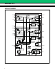
6 CSCP C21 1000 pF Charging current (1 mA) H priority L priority − + + Error Amp2 L priority − + + Error Amp1 12 13 CT C1 100 pF H: UVLO release SCP Comp. + + − OSC UVLO RT R1 24 kΩ 8 SCP Logic H: at SCP 15 B VREF 100 kΩ 13 kΩ R14 CS2 10 µA CH2 ON/OFF signal 68 kΩ 14 (Hiz : ON, L : OFF) C17 R13 0.1 220 1.24 V µF kΩ C14 16 VIN 1000 pF FB2 (7 V to 19 V) 19 DTC2 R15R16 −INE2 DTC1 R10R11 −INE1 10 A VREF 150 kΩ 56 kΩ R9 10 µA CS1 CH1 ON/OFF signal 68 kΩ 11 C16 R8 (Hiz : ON, L : OFF) 0.
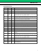
MB39A104 ■ PARTS LIST COMPONENT ITEM SPECIFICATION VENDOR PARTS No. Q1, Q2 Pch FET VDS = −30 V, ID = −6 A TOSHIBA TPC8102 D1, D2 Diode VF = 0.42 V (Max) , at IF = 3 A ROHM RB0530L-30 L1, L2 Inductor 15 µH 3.6 A, 50 mΩ SUMIDA CDRH104R-150 C1 C2, C6 C3, C7 C4, C8 C10, C11, C20 C12, C14, C21 C16, C17 Ceramics Condenser OS-CONTM Ceramics Condenser OS-CONTM Ceramics Condenser Ceramics Condenser Ceramics Condenser 100 pF 10 µF 10 µF 82 µF 0.1 µF 1000 pF 0.1 µF 50 V 20 V 25 V 6.
MB39A104 ■ SELECTION OF COMPONENTS • Pch MOS FET The P-ch MOSFET for switching use should be rated for at least 20% more than the maximum input voltage. To minimize continuity loss, use a FET with low RDS(ON) between the drain and source. For high input voltage and high frequency operation, on/off-cycle switching loss will be higher so that power dissipation must be considered. In this application, the Toshiba TPC8102 is used.
MB39A104 = ID 2 × RDS (ON) × Duty PC = 3 2 × 0.05 × 0.263 =: 0.118 W PS (ON) = = VD (Max) × ID × tr × fOSC 6 19 × 3 × 100 × 10−9 × 500 × 103 6 =: 0.475 W PS (OFF) = = VD (Max) × ID (Max) × tf × fOSC 6 19 × 3.25 × 100 × 10−9 × 500 × 103 6 =: 0.515 W PT = PC + PS (ON) + PS (OFF) =: 0.118 + 0.475 + 0.515 =: 1.108 W The above power dissipation figures for the TPC8102 are satisfied with ample margin at 2.4 W (Ta = +25 °C) . CH2 Input voltage VIN (Max) = 19 V output voltage VO = 3.
MB39A104 PC = ID 2 × RDS (ON) × Duty = 3 2 × 0.05 × 0.174 =: 0.078 W PS (ON) = VD (Max) × ID × tr × fOSC 6 = 19 × 3 × 100 × 10−9 × 500 × 103 6 =: 0.475 W PS (OFF) = = VD (Max) × ID (Max) × tf × fOSC 6 19 × 3.18 × 100 × 10−9 × 500 × 103 6 =: 0.504 W PT = PC + PS (ON) + PS (OFF) =: 0.078 + 0.475 + 0.504 =: 1.057 W The above power dissipation figures for the TPC8102 are satisfied with ample margin at 2.4 W (Ta = +25 °C) .
MB39A104 Example: CH1 L ≥ ≥ 2 (VIN − VO) ton IO 2 × (19 − 5) 1 × × 0.263 IO 500 × 103 ≥ 4.91 µH CH2 L ≥ ≥ 2 (VIN − VO) ton IO 2 × (19 − 3.3) 1 × × 0.174 IO 500 × 103 ≥ 3.64 µH Inductance values derived from the above formulas are values that provide sufficient margin for continuous operation at maximum load current, but at which continuous operation is not possible at light loads. It is therefore necessary to determine the load level at which continuous operation becomes possible.
MB39A104 To determine whether the current through the inductor is within rated values, it is necessary to determine the peak value of the ripple current as well as the peak-to-peak values of the ripple current that affect the output ripple voltage. The peak value and peak-to-peak value of the ripple current can be determined by the following formulas.
MB39A104 • Flyback diode The flyback diode is generally used as a Shottky barrier diode (SBD) when the reverse voltage to the diode is less than 40V. The SBD has the characteristics of higher speed in terms of faster reverse recovery time, and lower forward voltage, and is ideal for achieving high efficiency.
MB39A104 • Smoothing Capacitor The smoothing capacitor is an indispensable element for reducing ripple voltage in output. In selecting a smoothing capacitor it is essential to consider equivalent series resistance (ESR) and allowable ripple current. Higher ESR means higher ripple voltage, so that to reduce ripple voltage it is necessary to select a capacitor with low ESR.
MB39A104 CH2 ∆VO ∆IL ESR ≤ − 0.033 0.364 ≤ 1 2πfCL − 1 2π × 500 × 103 × 82 × 10−6 ≤ 86.8 mΩ Capacitance value CH1 CL ≥ ≥ ∆IL 2πf (∆VO − ∆IL × ESR) 0.491 2π × 500 × 103 × (0.050 − 0.491 × 0.05) ≥ 6.14 µF CH2 CL ≥ ≥ ∆IL 2πf (∆VO − ∆IL × ESR) 0.364 2π × 500 × 103 × (0.033 − 0.364 × 0.05) ≥ 7.83 µF Ripple current CH1 ICLrms ≥ ≥ (VIN − VO) ton 2√3L (19 − 5) × 0.263 2√3 × 15 × 10−6 × 500 × 103 ≥ 141.7 mArms CH2 ICLrms ≥ ≥ (VIN − VO) ton 2√3L (19 − 3.3) × 0.174 2√3 × 15 × 10−6 × 500 × 103 ≥ 105.
MB39A104 ■ REFERENCE DATA TOTAL Efficiency vs. Input Voltage 100 TOTAL efficiency η (%) 90 80 70 Vin = 7 V Vin = 10 V Vin = 12 V Vin = 19 V 60 Ta = +25 °C 5 V Output SW1 = OFF SW2 = ON 50 40 30 10 m 100 m 1 10 Input voltage VIN (V) Each CH Efficiency vs. Input Voltage 100 Each CH efficiency η (%) 90 80 70 Vin = 7 V Vin = 10 V Vin = 12 V Vin = 19 V 60 Ta = +25 °C 3.
MB39A104 (Continued) Switching Wave Form (CH1) VG (V) Ta = +25 °C VIN = 12 V CTL = 5 V VO = 5 V RL = 1.67 Ω 15 10 5 VS (V) 0 15 10 5 0 0 1 2 3 4 5 6 7 8 9 10 t (µs) Switching Wave Form (CH2) VG (V) Ta = +25 °C VIN = 12 V CTL = 5 V VO = 3.3 V RL = 1.
MB39A104 ■ USAGE PRECAUTION • Printed circuit board ground lines should be set up with consideration for common impedance. • Take appropriate static electricity measures. • Containers for semiconductor materials should have anti-static protection or be made of conductive material. • After mounting, printed circuit boards should be stored and shipped in conductive bags or containers. • Work platforms, tools, and instruments should be properly grounded.
MB39A104 ■ PACKAGE DIMENSIONS Note 1) *1 : Resin protrusion. (Each side : +0.15 (.006) MAX) . Note 2) *2 : These dimensions do not include resin protrusion. Note 3) Pins width and pins thickness include plating thickness. Note 4) Pins width do not include tie bar cutting remainder. 24-pin plastic SSOP (FPT-24P-M03) 0.17±0.03 (.007±.001) *17.75±0.10(.305±.004) 24 13 *2 5.60±0.10 7.60±0.20 (.220±.004) (.299±.008) INDEX Details of "A" part +0.20 1.25 –0.10 +.008 .049 –.004 (Mounting height) 0.25(.
MB39A104 FUJITSU LIMITED All Rights Reserved. The contents of this document are subject to change without notice. Customers are advised to consult with FUJITSU sales representatives before ordering.