Prelminary 2004.11.12 FUJITSU SEMICONDUCTOR DATA SHEET 32-Bit Proprietary Microcontroller LSI Network Security System MB91401 ■ DESCRIPTION The MB91401 is a network security LSI incorporating a Fujitsu’s 32-bit, FR-family RISC microcontroller with 10/ 100Base-T MAC Controller, encryption function and authentication function.
MB91401 Prelminary 2004.11.12 • For DES-ECB/DES-CBC/3DES-ECB/3DES-CBC mode* • For MD5/SHA-1/HMAC-MD5/HMAC-SHA-1 mode • DH group: for 1 (MODP 768 bit) /2 (1024 bit) For the encryption/authentication macros, a software library is available by contacting the Fujitsu sales representative as required. * : Encryption function (DES/3DES) Method to encrypt, and to decrypt plaintext in 64 bits with code and decoding key to 56 bits. (3DES is repeated three times. The key can be set by 168 bits or less.
Prelminary 2004.11.12 MB91401 (Continued) • CARD Interface (CompactFlash) The CompactFlash interface is a memory and I/O mode correspondence. It corresponds to the I/O of data such as not only the memory card but also the communication cards.
Prelminary 2004.11.
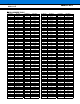
Prelminary 2004.11.12 MB91401 ■ PIN NUMBER TABLE Pin Number Pin name Pin Number Pin name Pin Number Pin name Pin Number 1 VSS 61 UDP 121 EXD11 181 Pin name SDA 2 CFD15 62 CFWEX 122 EXD14 182 USBINS 3 ICLK 63 CFCE1X 123 CFCD2X 183 UDM 4 ICS0 64 CFIORDX 124 UCLKSEL 184 CFRESET 5 TDI 65 CFA1 125 CFWAITX 185 CFREGX 6 UCLK48 66 CFA5 126 N.C.
Prelminary 2004.11.
Prelminary 2004.11.12 MB91401 SYSTEM (9 pin) Pin name Pin no. Polarity XINI 8 I/O Circuit Function/application IN D Clock input pin Input pin of clock generated in clock generator. 10 MHz to 50 MHz frequency can be input. INITXI 204 Negative IN D Reset input pin This pin inputs a signal to initialize the LSI. When turning on the power supply, apply “0” to the pin until the clock signal input to the CLKIN pin becomes stable.
Prelminary 2004.11.12 MB91401 ICE (9 pin) Pin name Pin no. Polarity I/O Circuit Function/application BREAKI 76 IN D Emulator break request pin This pin inputs the emulator break request when an ICE is connected. ICS2 ICS1 ICS0 74 75 4 OUT F Emulator chip status pins These pins output the emulator status when an ICE is connected. ICLK 3 I/O B Emulator clock pin This pin serves as the emulator clock pin when an ICE is connected.
Prelminary 2004.11.12 UART (6 pin) Pin name MB91401 Pin no. Polarity I/O Circuit SIN1 SIN0 85 15 IN D Serial data input pins Serial data input pin of UART built-in FR core. SOUT1 SOUT0 149 86 OUT F Serial data output pins Serial data output pin of UART built-in FR core. SCK1 SCK0 148 14 I/O B Serial clock I/O pins Serial clock input/output pin of UART built-in FR core. Polarity I/O Circuit OUT B MEMORY IF (66 pin) Pin name Pin no.
Prelminary 2004.11.12 MB91401 (Continued) Pin name 10 Pin no. Polarity I/O Circuit Function/application D31 D30 D29 D28 D27 D26 D25 D24 D23 D22 D21 D20 D19 D18 D17 D16 D15 D14 D13 D12 D11 D10 D9 D8 D7 D6 D5 D4 D3 D2 D1 D0 169 110 168 109 42 218 167 108 41 166 107 40 106 39 38 105 36 165 104 35 164 103 34 216 163 102 33 162 101 32 100 31 I/O B Data input/output pins 32 bits data input/output signal pin.
Prelminary 2004.11.12 MB91401 ETHERNET MAC CONTROLLER (17 pin) Pin name Pin no. Polarity I/O Circuit Function/application RXCLK 48 IN D Clock input for reception pin MII sync signal during reception. The frequency is 2.5 MHz at 10 Mbps and 25 MHz at 100 Mbps. RXER 113 Positive IN D Receive error input pin It is recognized that there is an error in the reception packet when “1” is input from the PHY device at receiving.
Prelminary 2004.11.12 MB91401 EXTERNAL IF (23 pin) Pin name Pin no. EXCSX 12 50 Polarity I/O Circuit Function/application Negative IN D External chip select input pin Chip select input pin from external host. EXA 116 IN D External address input pin Address input pin from external host.
Prelminary 2004.11.12 USB IF (5 pin) Pin name UDP MB91401 Pin no. 61 Polarity I/O I/O Circuit Function/application C USB data D + (differential) pin I/O signal pin on the plus side of the USB data. Use the LSI with 25 Ω to 30 Ω (27 Ω recommended) external series load resistors, 1.5 kΩ pull-up resistors and about 100 kΩ resistors. Input “0” when the USB macro is unused. UDM 183 I/O C USB data D − (differential) pin I/O signal pin on the minus side of the USB data.
Prelminary 2004.11.12 MB91401 CARD IF (41 pin) Pin name Pin no.
Prelminary 2004.11.12 (Continued) Pin name CFCD1X CFVS1X CFRDY (CFIREQ) CFWAITX MB91401 Pin no. Polarity 58 Negative 230 60 125 Negative Positive (Negative) Negative I/O IN IN IN IN Circuit Function/application E Card connection detect input pin : CFCD1X Checking connection pin of the socket and CompactFlash card. It is shown that the CompactFlash card was connected when this signal and CFCD2X are both input by “0”.
Prelminary 2004.11.12 MB91401 I2C IF (2 pin) Pin name Pin no. Polarity I/O Circuit SDA 181 I/O B Serial data line input/output pin I2C bus data I/O pin SCL 59 I/O B Serial clock line input/output pin I2C bus clock I/O pin Power Supply/GND (39 pin) Pin name Pin no. Polarity 16 I/O Circuit Function/application Function/application PLLVDD 199 Power supply V-E APLL dedicated power supply pin This pin is for 1.8 V power supply pin.
Prelminary 2004.11.12 MB91401 ■ I/O CIRCUIT TYPE Type Circuit Remarks Digital output A Digital output • • • • With pull/down CMOS level output CMOS level input Value of pull-down resistance = approx.
Prelminary 2004.11.12 MB91401 (Continued) Type D Circuit Remarks Digital input E Digital input CMOS level input • With pull-up • CMOS level input • Value of pull-up resistance = approx.
Prelminary 2004.11.12 MB91401 ■ HANDLING DEVICES Preventing Latch-up When a voltage that is higher than VDDE and a voltage that is lower than VSS are impressed to the input terminal and the output terminal in CMOS IC or the voltage that exceeds ratings between VDDE to VSS is impressed, the latch-up phenomenon might be caused. If latch-up occurs, the supply current increases rapidly, sometimes resulting in thermal breakdown of the device.
Prelminary 2004.11.12 MB91401 Figure When you share the power supply for digital and for VCO VDD (for digital) LSI PLLVDD (for VCO) APLL Power supply (a) Logic part PLLVSS VSS Treatment of the unused pins Leaving unused input pins open results in a malfunction, so process the pull-up or pull-down. Treatment of OPEN pins Be sure to use open pins in open state.
Prelminary 2004.11.12 MB91401 ■ CONNECTED SPECIFICATION OF MB91401 AND ICE Recommended type and circuit configuration of the emulator interface connector mounting on the user system, attention when designing and wiring regulation are shown. When the flat cable is used, the combination of the connectors with housing should be selected. Recommended connector type Attached cable FPC cable Part number Remarks FH10A-30S-1SH (Maker : Hirose Electric Co., Ltd.
Prelminary 2004.11.12 MB91401 • Precaution when designing When evaluation MCU on the user system is operated in the state that the emulator is not connected, should be treated as follow each input terminal of evaluation MCU connected with the emulator interface on the user system. Therefore, note that the switch circuit etc, might become necessary in the user system when you design. The terminal processing in each emulator interface is shown as follows.
Prelminary 2004.11.12 MB91401 JTAG The JTAG function is installed in this LSI. Note that the terminal INITXI should be input in "L" when using JTAG. Notes when quartz vibrator is mounted The crystal oscillation circuit built into this LSI operates by the following compositions.
Prelminary 2004.11.12 MB91401 • Reference Value Oscillation frequency C1, C2 C3 L Rr to 30 MHz 5 pF to 33 pF None None None 20 MHz to 50 MHz 5 pF to 15 pF 10 nF approx. 1 µH approx. None It is necessary to add C3/L depending on a basic wave and the over tone characteristic of the oscillator of the 20 MHz to 30 MHz belt. Note : These reference values are standards. The constant changes according to the characteristic of the quartz vibrator used.
Prelminary 2004.11.12 MB91401 • Notes as device Treatment of Unused Input Pins It causes the malfunction that the unused input terminal is made open, and do the processing such as 1 stack or 0 stacks. About Mode pins (MDI2 to MDI0) Connect these pins with the input buffer by 1 to 1 to prevent the malfunction by the noise, and connect directly to VDD or VSS outside of ASIC. Operation at start-up Specify set initialization reset (INIT) with the terminal INITXI when you turn on the power supply.
MB91401 Prelminary 2004.11.12 CPU • The instruction fetch is not done from D-bus, and does not set the code area on D-bus RAM. • Set neither stack area nor the vector table on the instruction RAM. • The following operations may be performed when the instruction immediately followed by a DIVOU/DIVOS instruction is (a) halted by a user interrupt or NMI, (b) single-stepped, or (c) breaks in response to a data event or emulator menu: (1) The D0 and D1 flags are updated in advance.
Prelminary 2004.11.12 MB91401 • External bus interface • When the bus width of the area set up as little endian is 32-bit, confine to word (32-bit) access when accessing the relevant area. • When enabling prefetch to the area set to the Little endian, give the access to the corresponding area as word (32 bits) access limitation. In the byte and the half word access, it is not possible to access it correctly. • DMA • Do not transfer DMA to instruction RAM.
Prelminary 2004.11.12 MB91401 ■ NOTES OF DEBUG Step execution of RETI instruction In an environment where interrupts frequently occur during single-step execution, only the relevant interrupt processing routines are executed repeatedly during single-step execution of the RETI instruction. This will prevent the main routine and low-interrupt-level programs from being executed. Do not execute step of RETI instruction for escape.
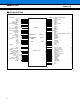
Prelminary 2004.11.12 MB91401 ■ BLOCK DIAGRAM FR core E I-Cach (4 KB) D-RAM (8 KB) R Serial IF (2ch) UART INT/NMI INT B DMAC OSC Crystal Unit CLK Cont CLKIN USB CLK (48 MHz) PLL Timer T Authentication macro IPsec Accelerator (IKE Accelerator) DES/3DES HMAC-MD5/SHA1 DSU LAN controller 10/100 Ethernet MAC Controller DSU IF PHY L3/L4 Filtering USB Function Rev2.0FS USB IF DH Ext.
Prelminary 2004.11.12 MB91401 ■ MEMORY SPACE • Memory space The FR family has 4 GByte of logical addresses (232 address) which can be linearly accessed by the CPU. Direct Addressing Areas The following address space areas are used as I/O areas. These areas are called direct addressing areas, in which the address of an operand can be specified directly during an instruction.
Prelminary 2004.11.12 MB91401 ■ GENERAL PURPOSE REGISTERS 32 bits Initial Value: R0 XXXX XXXXH R1 R12 R13 AC R14 FP XXXX XXXXH R15 SP 0000 0000H Registers R0 to R15 are general-purpose registers. The registers are used as the accumulator and memory access pointers for CPU operations. Of these 16 registers, the registers listed below are intended for special applications, for which some instructions are enhanced.
Prelminary 2004.11.12 MB91401 ■ MODE SETTINGS The FR family uses the mode pins (MDI2 to MDI0) and the mode register (MODR) to set the operation mode. • Mode Pins Three mode pins MDI[2], MDI[1], and MDI[0] are used to specify a mode vector fetch or test mode.
Prelminary 2004.11.12 MB91401 [bit1, bit0] WTH1, WTH0 (Bus width setting bits) These bits specify the bus width. The value of the bits is set in the DBW1 and DBW0 bits in ACR0 (CSO area). Set these bits to a value other than “11”. WTH1 WTH0 Function Remarks 0 0 8-bit bus width External bus mode 0 1 16-bit bus width External bus mode 1 0 32-bit bus width External bus mode 1 1 Setting disabled • Operation mode In the operation mode, there are a bus mode and an access mode.
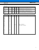
Prelminary 2004.11.12 MB91401 ■ I/O MAP This shows the location of the various peripheral resource registers in the memory space.
Prelminary 2004.11.
Prelminary 2004.11.
Prelminary 2004.11.
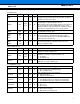
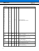
Prelminary 2004.11.12 MB91401 (Continued) Address Register +0 +1 0000_0684H +3 TCR [R/W] 00000000*1 Block 0000_067CH 0000_0680H +2 CSER [R/W] 00000001 CHER [R/W] XXXXXXX1 RCR 00XXXXXX 00XXXXXX Memory IF 0000_0688H to 0000_0FFCH Reserved *1 : An initial value is a different register at the reset level. The display is the one at the INIT level. *2 : An initial value is a different register at the reset level. The display is due to the INIT level by INITX.
Prelminary 2004.11.
Prelminary 2004.11.
Prelminary 2004.11.
Prelminary 2004.11.
Prelminary 2004.11.
Prelminary 2004.11.
Prelminary 2004.11.
Prelminary 2004.11.
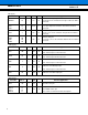
Prelminary 2004.11.12 MB91401 ■ ELECTRICAL CHARACTERISTICS 1. Absolute Maximum Ratings Parameter Symbol Rating Min Max Unit Remarks I/O VDDE VSS − 0.3 VSS + 4.0 V Internal VDDI VSS − 0.3 VSS + 2.5 V PLLVDD VSS − 0.3 VSS + 4.0 V Input voltage*1 VI VSS − 0.3 VDDE + 0.3 V Output voltage*1 VO VSS − 0.3 VDDE + 0.3 V “L” level maximum output current IOL T.B.D mA *3 “L” level average output current IOLAV T.B.D mA *4 “L” level total maximum output current ΣIOL T.
Prelminary 2004.11.12 MB91401 2. Recommended Operating Conditions Parameter Power supply voltage Value Min Typ Max Unit I/O VDDE 3.0 3.3 3.6 V Internal VDDI 1.65 1.8 1.95 V PLLVDD VSS + 3.0 VDDE V Ta − 10 70.0 °C Analog power supply voltage Operating temperature Symbol (VSS = PLLVSS = 0 V) WARNING: The recommended operating conditions are required in order to ensure the normal operation of the semiconductor device.
Prelminary 2004.11.12 MB91401 3. DC Characteristics • Other than USB (VSS = PLLVSS = 0 V) Symbol Pin Conditions “H” level input voltage VIH “L” level input voltage VIL “H” level output voltage VOH “L” level output voltage VOL Parameter Value Unit Min Typ Max 2.0 VDDE + 0.3 V VSS − 0.3 0.8 V VDDE = 3.0 V, IOH = 4.0 mA VDDE − 0.5 V VDDE = 3.0 V, IOH = 4.0 mA 0.4 V ILI VDDE = 3.
Prelminary 2004.11.12 MB91401 • USB (VSS = PLLVSS = 0 V) Symbol Pin “H” level output voltage VOH IOH = − 100 µA “L” level output voltage VOL IOL = 100 µA “H” level output current IOH “L” level output current IOL output short circuit current Input leak current Parameter Conditions Value Unit Remarks Min Typ Max VDDE − 0.2 VDDE V 0 0.2 V VOH = VDDE − 0.4 V − 20 mA VOL = 0.
Prelminary 2004.11.12 MB91401 USB Specification Revision 1.1 Parameter Symbol Value Min Max Unit Remarks Input Levels High (driven) VIH 2.0 V *1 Low VIL 0.8 V *1 Diffential Input Sensitivity VDI 0.2 V *2 Differential Common Mode Range VCM 0.8 2.5 V *2 High (driven) VOH 0.0 0.3 V *3 Low VOL 2.8 3.6 V *3 Output Signal Crossover Voltage VCRS 1.3 2.0 V *4 Bus Pull-up Resistor on Upstream Port RPU 1.425 1.
Prelminary 2004.11.12 MB91401 *4 :
Prelminary 2004.11.12 MB91401 4. AC Characteristics The following measurement conditions depending on the supply voltage apply to the MB91401 unless otherwise specified. • AC measurement condition Input Output VCC VIH VOH VIL VCC VOL 0V 0V VIH VDDE × 0.8 VOH VDDE/2 VIL VDDE × 0.
Prelminary 2004.11.12 MB91401 (2) Reset Symbol Pin Reset input time trstl INITXI PLL reset input time tprstl PLLS Parameter Conditions After power supply & input clock stabilization Max At unusing of PLL 5 tcp ns At using of PLL 600 + 1 µs At using of PLL 1 µs trstl, tprstl 54 Unit Remarks Min Note : tcp is internal CPU and clock cycle period for peripheral module.
Prelminary 2004.11.
Prelminary 2004.11.
Prelminary 2004.11.
Prelminary 2004.11.
Prelminary 2004.11.
Prelminary 2004.11.
Prelminary 2004.11.
Prelminary 2004.11.12 MB91401 (8) External IF • Read access Parameter Symbol Pin texrc EXA to Data Valid Value Max EXA, EXCSX 6 × tcp ns texadv EXA, EXD 5 × tcp ns EXCSX to Data Valid texcsdv EXCSX, EXD 5 × tcp ns EXRDX to Data Out Enable texdoe EXRDX, EXD 5 × tcp ns EXRDX “H” to High Z texdhz EXRDX, EXD 5 × tcp + 8 ns EX Read Cycle time Note : tcp is internal CPU and operational clock period for peripheral module.
Prelminary 2004.11.12 MB91401 • Write access Parameter Symbol Value Pin Min Max Unit EX Write Cycle time texwc EXA, EXCSX 5 × tcp ns EXA to Data Setup time texads EXA, EXD 4 × tcp ns EXCSX to Data Setup time texcsds EXCSX, EXD 4 × tcp ns EXWRX “L” Pulse width texwp EXRDX, EXD 4 × tcp ns EXD Setup time texds EXRDX, EXD 11 ns EXD Hold time texdh EXRDX, EXD 0 ns Remarks Note : tcp is internal CPU and operational clock period for peripheral module.
Prelminary 2004.11.12 MB91401 (9) USB interface Parameter Symbol Pin Input clock tucyc RISE Time Fall Time Value Unit Remarks Min Typ Max UCLK48 48*1 tutfr UDP, UDM 4 20 ns *2 tutff UDP, UDM 4 20 ns *2 Differential Rise and Fall Timing Matching tutfrfm UDP, UDM 90 111.
Prelminary 2004.11.12 MB91401 Full-speed Buffer Rs 28 Ω to 44 Ω Equiv. Imped T×D+ CL = 50 pF Rs 28 Ω to 44 Ω Equiv.
Prelminary 2004.11.12 MB91401 (10) I2C interface • Input timing specification Parameter Symbol Pin SDA input setup time ts2sdai SDA input hold time Value Unit Remarks Min Max SDA 250 ns * th2sdai SDA 0 ns * tcscli SCL 10 µs * SCL input “H” pulse time twhscli SCL 4 µs * SCL input “L” pulse time twlscli SCL 4.7 µs * SCL input setup time ts2scli SCL 4 µs * SCL input hold time th2scli SCL 4.
Prelminary 2004.11.
Prelminary 2004.11.
Prelminary 2004.11.
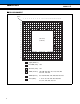
Prelminary 2004.11.12 MB91401 ■ PACKAGE DIMENSION 240-pin plastic FBGA (BGA-240P-M01) Note: The actual shape of coners may differ from the dimension. 240-¯0.30±0.10 (240-¯.012±.004) 10.00±0.10(.394±.004)SQ +0.20 Ð0.10 +.008 Ð.004 1.13 .044 (Mounting height) 0.10(.004) (INDEX AREA) 0.05(.002) M 0.50(.020) TYP 9.00(.354) REF INDEX 19 18 17 16 15 14 13 12 11 10 9 8 7 6 5 4 3 2 1 WV U T R P NM L K J HG F E D C B A 0.25±0.10 (.010±.
Prelminary 2004.11.
Prelminary 2004.11.12 MB91401 FUJITSU LIMITED For further information please contact: Japan FUJITSU LIMITED Marketing Division Electronic Devices Shinjuku Dai-Ichi Seimei Bldg. 7-1, Nishishinjuku 2-chome, Shinjuku-ku, Tokyo 163-0721, Japan Tel: +81-3-5322-3353 Fax: +81-3-5322-3386 http://edevice.fujitsu.com/ North and South America FUJITSU MICROELECTRONICS AMERICA, INC. 1250 E. Arques Avenue, M/S 333 Sunnyvale, CA 94088-3470, U.S.A. Tel: +1-408-737-5600 Fax: +1-408-737-5999 http://www.fma.fujitsu.