
Datasheet
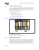

Intel® Xeon™ Processor with 800 MHz System Bus
16 Datasheet
Table 12 for the DC specifications for these signals. A minimum voltage is provided in Table 9 and
changes with frequency. This allows processors running at a higher frequency to have a relaxed
minimum voltage specification. The specifications have been set such that one voltage regulator
can operate with all supported frequencies.
Individual processor VID values may be calibrated during manufacturing such that two devices at
the same core speed may have different default VID settings. This is reflected by the VID Range
values provided in Table 9. Refer to the Intel® Xeon™ processor with 800 MHz System Bus
Specification Update for Specification Update for further details on specific valid core frequency
and VID values of the processor.
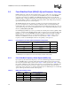
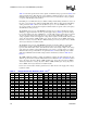
The Intel® Xeon™ processor with 800 MHz system bus uses six voltage identification signals,
VID[5:0], to support automatic selection of power supply voltages. Table 4 specifies the voltage
level corresponding to the state of VID[5:0]. A ‘1’ in this table refers to a high voltage level and a
‘0’ refers to a low voltage level. If the processor socket is empty (VID[5:0] = x11111), or the
voltage regulation circuit cannot supply the voltage that is requested, it must disable itself. See the
Voltage Regulator Module (VRM) and Enterprise Voltage Regulator-Down (EVRD) 10.0 Design
Guidelines or Voltage Regulator Module (VRM) and Enterprise Voltage Regulator-Down (EVRD)
10.1 Design Guidelines for further details.
The Intel® Xeon™ processor with 800 MHz system bus provides the ability to operate while
transitioning to an adjacent VID and its associated processor core voltage (V
CC
). This will
represent a DC shift in the load line. It should be noted that a low-to-high or high-to-low voltage
state change may result in as many VID transitions as necessary to reach the target core voltage.
Transitions above the specified VID are not permitted. Table 9 includes VID step sizes and DC
shift ranges. Minimum and maximum voltages must be maintained as shown in Table 10 and
Figure 4.
The VRM or VRD used must be capable of regulating its output to the value defined by the new
VID. DC specifications for dynamic VID transitions are included in Table 9 and Table 10. Please
refer to the Voltage Regulator Module (VRM) and Enterprise Voltage Regulator-Down (EVRD)
10.0 Design Guidelines or Voltage Regulator Module (VRM) and Enterprise Voltage Regulator-
Down (EVRD) 10.1 Design Guidelines for further details.
Power source characteristics must be guaranteed to be stable whenever the supply to the voltage
regulator is stable.
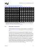
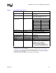
Table 4. Voltage Identification Definition (Sheet 1 of 2)
2,3
VID5 VID4 VID3 VID2 VID1 VID0 V
CC_MAX
VID5 VID4 VID3 VID2 VID1 VID0 V
CC_MAX
0010100.8375 0 1 1 0 1 0 1.2125
1010010.8500
1 1 1 0 0 1 1.2250
0010010.8625
0 1 1 0 0 1 1.2375
1010000.8750
1 1 1 0 0 0 1.2500
0010000.8875
0 1 1 0 0 0 1.2625
1001110.9000
1 1 0 1 1 1 1.2750
0001110.9125
0 1 0 1 1 1 1.2875
1001100.9250
1 1 0 1 1 0 1.3000
0001100.9375
0 1 0 1 1 0 1.3125
1001010.9500
1 1 0 1 0 1 1.3250
0001010.9625
0 1 0 1 0 1 1.3375
1001000.9750
1 1 0 1 0 0 1.3500
0001000.9875
0 1 0 1 0 0 1.3625
1000111.0000
1 1 0 0 1 1 1.3750