
Datasheet

Intel® Xeon™ Processor with 800 MHz System Bus
46 Datasheet
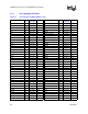
TCK I TCK (Test Clock) provides the clock input for the processor Test Bus (also known as the
Test Access Port).
TDI I TDI (Test Data In) transfers serial test data into the processor. TDI provides the serial
input needed for JTAG specification support.
TDO O TDO (Test Data Out) transfers serial test data out of the processor. TDO provides the
serial output needed for JTAG specification support.
TEST_BUS I/O Must be connected to all other processor TEST_BUS signals in the system.
TESTHI[6:0] I All TESTHI inputs should be individually connected to V
TT
via a pull-up resistor which
matches the trace impedance. TESTHI[3:0] and TESTHI[6:5] may all be tied together
and pulled up to V
TT
with a single resistor if desired. However, usage of boundary scan
test will not be functional if these pins are connected together. TESTHI4 must always be
pulled up independently from the other TESTHI pins. For optimum noise margin, all pull-
up resistor values used for TESTHI[6:0] should have a resistance value within ±20% of
the impedance of the baseboard transmission line traces. For example, if the trace
impedance is 50 Ω, than a value between 40 Ω and 60 Ω should be used.
THERMDA Other Thermal Diode Anode. See Section 6.2.7.
THERMDC Other Thermal Diode Cathode. See Section 6.2.7.
THERMTRIP# O Assertion of THERMTRIP# (Thermal Trip) indicates the processor junction temperature
has reached a temperature beyond which permanent silicon damage may occur.
Measurement of the temperature is accomplished through an internal thermal sensor.
Upon assertion of THERMTRIP#, the processor will shut off its internal clocks (thus
halting program execution) in an attempt to reduce the processor junction temperature.
To protect the processor its core voltage (V
CC
) must be removed following the assertion
of THERMTRIP#.
Driving of the THERMTRIP# signals is enabled within 10 ms of the assertion of
PWRGOOD and is disabled on de-assertion of PWRGOOD. Once activated,
THERMTRIP# remains latched until PWRGOOD is de-asserted. While the de-assertion
of the PWRGOOD signal will de-assert THERMTRIP#, if the processor’s junction
temperature remains at or above the trip level, THERMTRIP# will again be asserted
within 10 ms of the assertion of PWRGOOD.
2
TMS I TMS (Test Mode Select) is a JTAG specification support signal used by debug tools.
This signal does not have on-die termination and must be terminated at the end agent.
TRDY# I TRDY# (Target Ready) is asserted by the target to indicate that it is ready to receive a
write or implicit writeback data transfer. TRDY# must connect the appropriate pins of all
front side bus agents.
TRST# I TRST# (Test Reset) resets the Test Access Port (TAP) logic. TRST# must be driven low
during power on Reset.
V
CCA
IV
CCA
provides isolated power for the analog portion of the internal processor core PLLs.
V
CCIOPLL
IV
CCIOPLL
provides isolated power for digital portion of the internal processor core PLLs.
V
CCPLL
I The on-die PLL filter solution will not be implemented on this platform. The V
CCPLL
input
should left unconnected.
VCCSENSE
VSSSENSE
O VCCSENSE and VSSSENSE provide an isolated, low impedance connection to the
processor core power and ground. They can be used to sense or measure power near
the silicon with little noise.
VID[5:0] O VID[5:0] (Voltage ID) pins are used to support automatic selection of power supply
voltages (V
CC
). These are open drain signals that are driven by the processor and must
be pulled up through a resistor. Conversely, the VR output must be disabled prior to the
voltage supply for these pins becomes invalid. The VID pins are needed to support
processor voltage specification variations. See Table 4 for definitions of these pins. The
VR must supply the voltage that is requested by these pins, or disable itself.
Table 20. Signal Definitions (Sheet 8 of 9)
Name Type Description Notes