
Manual

GE
Preliminary Data Sheet
12A Digital SlimLynx
TM
: Non-Isolated DC-DC Power Modules
3Vdc –14.4Vdc input; 0.45Vdc to 5.5Vdc output; 12A Output Current
February 19, 2014 ©2014 General Electric Company. All rights reserved. Page 15
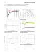
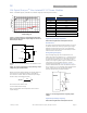
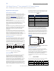
Figure 41. Output Voltage vs. Input Voltage Set Point Area
plot showing limits where the output voltage can be set for
different input voltages.
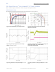
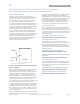
V
O
(+)
TRIM
VS
─
R
trim
LOAD
V
IN
(+)
ON/OFF
VS+
SIG_GND
Caution –
Do not connect SIG_GND to GND elsewhere in the
layout
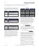
Figure 42. Circuit configuration for programming output
voltage using an external resistor.
Without an external resistor between Trim and SIG_GND pins,
the output of the module will be 0.6Vdc.To calculate the
value of the trim resistor,
Rtrim
for a desired output voltage,
should be as per the following equation:
()
Ω
−
= k
Vo
Rtrim
6.0
12
Rtrim is the external resistor in k
Vo
is the desired output voltage.
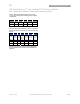
Table 1 provides Rtrim values required for some common
output voltages.
Table 1
V
O, set
(V) Rtrim (K)
0.6 Open
0.9 40
1.0 30
1.2 20
1.5 13.33
1.8 10
2.5 6.316
3.3 4.444
5.0 2.727
Digital Output Voltage Adjustment
Please see the Digital Feature Descriptions section.
Remote Sense
The power module has a Remote Sense feature to minimize
the effects of distribution losses by regulating the voltage
between the sense pins (VS+ and VS-). The voltage drop
between the sense pins and the VOUT and GND pins of the
module should not exceed 0.5V.
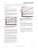
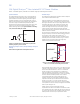
Analog Voltage Margining
Output voltage margining can be implemented in the
module by connecting a resistor, R
margin-up
, from the Trim pin
to the ground pin for margining-up the output voltage and
by connecting a resistor, R
margin-down
, from the Trim pin to
output pin for margining-down. Figure 43 shows the circuit
configuration for output voltage margining. The POL
Programming Tool, available at www.lineagepower.com
under the Downloads section, also calculates the values of
R
margin-up
and R
margin-down
for a specific output voltage and %
margin. Please consult your local GE Critical Power
technical representative for additional details.
Figure 43. Circuit Configuration for margining Output
voltage.
Digital Output Voltage Margining
Please see the Digital Feature Descriptions section.
0
2
4
6
8
10
12
14
16
0.511.522.533.544.555.56
Input Voltage (v)
Output Voltage (V)
Lower
Upper
Vo
MODULE
SIG_GND
Trim
Q1
Rtrim
Rmargin-up
Q2
Rmargin-down