
Manual

GE
Data Sheet
12V TLynx
TM
20A: Non-Isolated DC-DC Power Modules
4.5Vdc –14Vdc input; 0.69Vdc to 5.5Vdc output; 20A Output Current
May 2, 2013 ©2013 General Electric Company. All rights reserved. Page 16
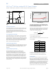
feature is not being used, connect the S+ pin to the VOUT pin
and the S– pin to the GND pin.
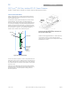
V
O
(+)
TRIM
GND
R
tr i m
LOAD
V
IN
(+)
ON/OFF
S+
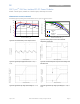
Figure 45. Circuit configuration for programming output
voltage using an external resistor.
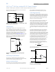
Voltage Margining
Output voltage margining can be implemented in the 12V
TLynx
TM
modules by connecting a resistor, R
margin-up
, from the
Trim pin to the ground pin for margining-up the output voltage
and by connecting a resistor, R
margin-down
, from the Trim pin to
output pin for margining-down. Figure 46 shows the circuit
configuration for output voltage margining. The POL
Programming Tool, available at www.lineagepower.com under
the Design Tools section, also calculates the values of R
margin-up
and R
margin-down
for a specific output voltage and % margin.
Please consult your local GE Technical Representative for
additional details.
Vo
MODULE
GND
Trim
Q1
Rtrim
Rmargin-up
Q2
Rmargin-down
Figure 46. Circuit Configuration for margining Output
voltage
Monotonic Start-up and Shutdown
The 12V TLynx
TM
modules have monotonic start-up and
shutdown behavior for any combination of rated input voltage,
output current and operating temperature range.
Startup into Pre-biased Output
The 12V Pico TLynx
TM
20A modules can start into a prebiased
output as long as the prebias voltage is 0.5V less than the set
output voltage. Note that prebias operation is not
supported when output voltage sequencing is used.
Output Voltage Sequencing
The 12V TLynx
TM
modules include a sequencing feature,
EZ-SEQUENCE that enables users to implement various
types of output voltage sequencing in their applications.
This is accomplished via an additional sequencing pin.
When not using the sequencing feature, either tie the
SEQ pin to V
IN or leave it unconnected.
When an analog voltage is applied to the SEQ pin, the
output voltage tracks this voltage until the output
reaches the set-point voltage. The final value of the SEQ
voltage must be set higher than the set-point voltage of
the module. The output voltage follows the voltage on
the SEQ pin on a one-to-one volt basis. By connecting
multiple modules together, multiple modules can track
their output voltages to the voltage applied on the SEQ
pin.
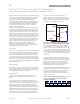
For proper voltage sequencing, first, input voltage is
applied to the module. The On/Off pin of the module is
left unconnected (or tied to GND for negative logic
modules or tied to V
IN for positive logic modules) so that
the module is ON by default. After applying input voltage
to the module, a minimum 10msec delay is required
before applying voltage on the SEQ pin. During this time,
a voltage of 50mV (± 20 mV) is maintained on the SEQ
pin. This delay gives the module enough time to
complete its internal power-up soft-start cycle. During
the delay time, the SEQ pin should be held close to
ground (nominally 50mV ± 20 mV). This is required to
keep the internal op-amp out of saturation thus
preventing output overshoot during the start of the
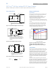
sequencing ramp. By selecting resistor R1 (see fig. 47)
according to the following equation
05.0
24950
1
−
=
IN
V
R
ohms,
the voltage at the sequencing pin will be 50mV when the
sequencing signal is at zero.
R1
GND
VIN+
SEQ
+
-
OUT
10K
499K
MODULE
Figure 47. Circuit showing connection of the
sequencing signal to the SEQ pin.