
Owner's manual


G
S
3
C
T
p
OUTPUT VOLTAGE
On/Off VOLTAGE
G
E
S
STW00
3
6-75Vdc I
n
March 26, 2013
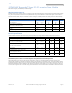
C
haracteri
s
T
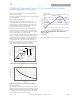
he following fi
p
ositive or neg
a
EFFICIENCY, (%)
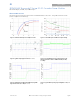
Figure 1. Con
v
OUTPUT VOLTAGE
V
O
(V) (100mV/div)
Figure 3. Typ
i
OUTPUT VOLTAGE
On/Off VOLTAGE
V
O
(V) (1V/div) V
On/Off
(V) (2V/div)
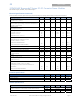
Figure 5.Typi
c
logic version
5A0F Ba
n
put; 3.3V
d
s
tic Curve
s
gures provide
a
tive remote
O
OUT
P
verter Efficie
n
T
i
cal output rip
T
c
al Start-up U
s
shown (V
IN
=
4
rracuda
d
c, 5A, 15
W
©
s
typical charac
O
n/Off logic.
P
UT CURRENT, I
O
n
cy versus Ou
t
T
IME, t (2
s/div)
ple and noise
T
IME, t (5ms/div)
s
ing Remote
O
4
8V, Io = I
o,max
)
™ Serie
s
W
Output
©
2012 General
E
teristics for th
e
(A)
t
put Current.
(I
o
= I
o,max
).
O
n/Off, negati
v
.
s
; DC-D
C
lectric Compan
y
e
SSTW005A0
F
INPUT CURRENT, I
IN
(A)
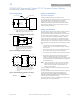
Figu
r
OUTPUT CURRENT OUTPUT VOLTAGE
Io(A) (2A/div) V
O
(V) (100mV/div)
Figu
r
Cha
n
C
O
>1
OUTPUT VOLTAGE INPUT VOLTAGE
V
O
(V) (1V/div) V
IN
(V) (
2
0V/div)
v
e Figu
r
I
o,max
)
C
Conver
t
y
. All rights reser
v
F
(3.3V, 5A) at 2
r
e 2. Convert
e
r
e 4. Transien
t
n
ge from 50%
00μF
V
O
(V) (1V/div) V
IN
(V) (
2
0V/div)
r
e 6. Typical S
t
)
.
t
er Pow
e
v
ed.
5
o
C. The figur
e
INPUT V
O
e
r Input Curre
n
TIME,
t
t
Response to
to 75% to 50
%
TIME,
t
t
art-up Using
Data S
h
e
r Modu
e
s are identica
O
LTAGE, V
IN
(V)
n
t versus Inpu
t
(1ms/div)
0.1A/µS Dyna
%
of full load,
V
t
(5ms/div)
Input Voltag
e
h
eet
les
Pag
e
l for either
t Voltage.
mic Load
V
in=48V,
e
(V
IN
= 48V, I
o
=
e
5
=