
User's Manual


GPA-1 manual
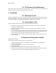
Figure1–J104andR112Locations
2 Interfaces
2.1 J101ControlInterface
TheJ101ControlInterfaceisintendedtoconnecttothetransceiver’scontrolinterfaceandprovides
keyingandpowercontrolsignals.
Table1–J101ControlCablePinFunctions
Pin Function
Pin1 3VdcenableTX,low=off
Pin2 0.7Vdc(variestosetRFpower)
Pin3 Notused
Pin4 Ground
2.2 J102RFOutput
J102isa50OhmFemaleTypeNconnector.
2.3 J103RFInput
J103isa50OhmMaleTypeN,REVERSEPolarityconnector.ThisRFampisprovidedwithaReverse
PolarityNconnector,tomeettheFCCRFsignalBooster/Amplifierrules.Theconnectorisprovidedsothat
onlyoneRFsignalcanbeinputtotheRFAmp.
Thisamplifierisdesigned
tobeonlyusedwiththeGEMDSSD1DataTransceiver.
AtnotimeshallthisamplifierbeusedwithnomorethantheintendedsingleRFinput,anyother
combinationofsignalshallvoidtheFCCtypeapprovalofthisamplifier
2.4 J104External/InternalJumper
J104isajumperblockwith3pins.Shortingpins1and2(EXT)isnotusedfortheGPA‐1.Shortingpins2
and3(INT)enablestheamplifier’sinternalpowerdetectortocontroltheamplifierpoweroutput.Access
tothisjumperblockisviaaholeinthetop
cover.