GE Sensing & Inspection Technologies SOLDER JOINT INSPECTION AND ANALYSIS with phoenix|x-ray microfocus and nanofocus X-ray systems
FAQs about X-ray How X-ray inspection source large FOD works object FDD detector high magnification low magnification insulator UH UG cathode (filament) UACC grid anode deflection unit electron beam magnetic lens X-ray starts with a sample being irradiated by an X-ray source and projected onto a detector. The geometric magnification M of the image is the ratio of focus-detector distance (FDD), Focus-object distance (FOD): M=FDD/FOD. The smaller the focal spot, the greater the resolution.
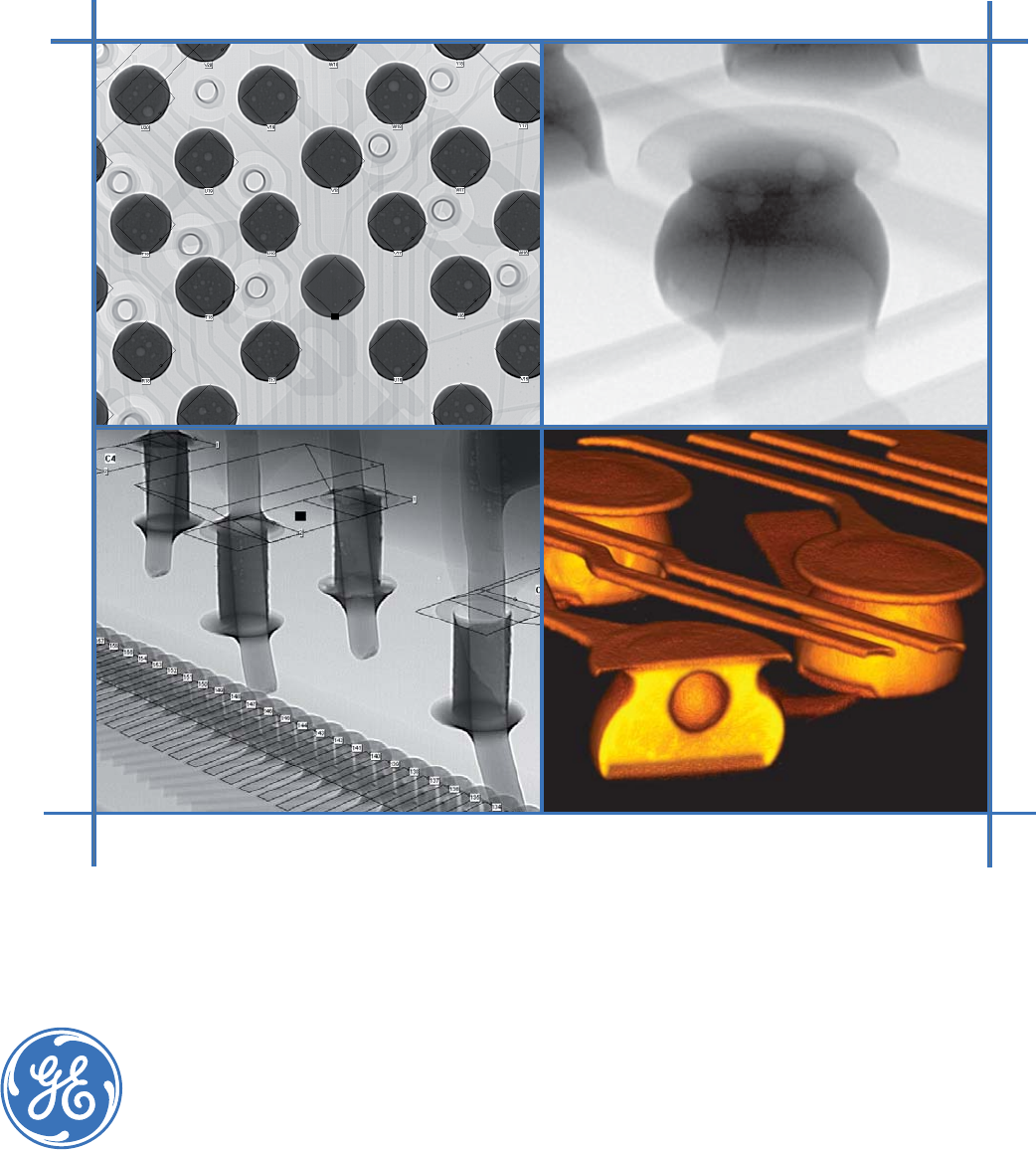
The View Inside Why to inspect solder joints with X-ray? The reliability of electronic assemblies strongly depends on solder joint quality. Acceptability criteria are mainly based on shape and dimension of the solder joints. As quality demands and technology for assembly process for new package types increase, many solder joints are no longer directly visible. Fortunately, they can easily be inspected by advanced microfocus and nanofocus X-ray systems.
The Third Dimension Just look from the side ovhm - oblique views at highest magnification Some acceptability criteria refer to a side view and many defects can be seen best from the side, in other words, some information about the vertical dimension is required. phoenix|x-ray systems provide this information by oblique view―up to 70 degrees―at highest magnification. As an example, this enables the user to see open BGA solder joints directly instead of interpreting signatures.
Automated Inspection The efficient way of process control and rework Efficient soldering process control requires the acquisition of statistical data on the solder joints of a larger number of samples. phoenix|x-ray offers a range of plug-in software modules for the automatic evaluation of standard solder joints like BGA, QFP, QFN, or PTH. For non-typical interconnections, appropriate modules can quickly be customised with the XE² (X-ray image Evaluation Environment) software.
Anticipating the Future Inspecting the smallest and finest nanofocus and digital imaging Miniaturisation and new assembly tech- High-resolution 3D-imaging niques demand resolution in the submicron range and also highest contrast resolution. With the nanofocus tube technology together with digital image chains or the fully digital high|contrast40 micron solder bumps at nanofocus resolution detector (up to 16 bit) phoenix|x-ray provides proven detail detectability down to 200 nm (0.
Systems phoenix|x-ray offers a wide range of systems and system configurations dedicated to various inspection tasks in printed circuit board assembly: nanome|x microme|x the ultimate X-ray solution automated solder joint inspection This automated X-ray system with superior speci- The microme|x is a high-resolution au- fications satisfies even the highest demands: The tomated X-ray inspection (AXI) system 180 kV / 15 W high-power nanofocus tube (4-in-1) that is suitable for failure analysis in the
Regional Contact Information Europe, Asia, Africa, South America GE Sensing & Inspection Technologies Niels-Bohr-Str. 7 31515 Wunstorf P.O. Box 6241 31510 Wunstorf Germany Tel.: +49 5031 172 0 Fax: +49 5031 172 299 E-mail: phoenix-info@ge.com phoenix-asia@ge.com Americas GE Sensing & Inspection Technologies 50 Industrial Park Road Lewistown, PA 17044 Tel: +1 (866) 243 2638 (toll-free) Tel: +1 (717) 447 1562 E-mail: phoenix-usa@ge.com www.phoenix-xray.