
Integration Guide

OEM TD-CDMA PCI Express Module Integration
May 2013 General Dynamics Broadband Proprietary and Confidential Page 15 of 20
Subject to Non Disclosure Agreement
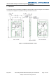
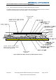
4.1.3 Physical Thermal Arrangement – PEM and Adaptor
This section describes the thermal arrangement of the PEM and Adaptor assembly.
The arrangement is architected to maximize the heat transfer from the PEM to the Adaptor Card by
creating a low thermal resistance between the PEM and the Adapter board. A similar scheme will be
described for laptop installations.
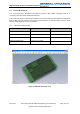
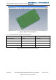
a) The layer structure of PCB – PEM see section 3.1 above, to spread heat to use the full
surface area of the PCB.
b) The layer structure of PCB – PEM Adaptor see section 3.2 above, to spread heat to use the
full surface area of the PCB and to provide a thermal conduction path through the base of the
enclosure.
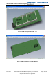
c) Use of a graphite thermal spreader material on top of top shielding can.
d) Use of an aluminium foil unit label covers top of unit and facilitates conduction and spreader
on the top surface of the PEM unit assembly.
e) graphite spreader/interface material on bottom of bottom snapshot shield to interface between
bottom snapshot and adaptor board.
f) gaps between components and shielding cans are filled with thermal gasket in the short term,
longer term the shielding can shall be contoured in contact with the components.
g) thermal conduction through the 52way connector has also provided significant thermal
conduction path to the adaptor board.
h) thermal conduction through the SMT threaded mounting bosses on the TD-CDMA PEM
Adaptor PCB.