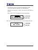
NT 250 Technical and Maintenance Manual NicomUsa Inc TABLE OF CONTENTS CHAPTER 1 Transmitter General Description And Installation Procedures Remote Control Feature Programming the NT 250 Page 2 Page 3 Page 5 CHAPTER 2 Electrical & Mechanical Specifications Front Panel Description Rear Panel Description Page 10 Page 13 Page 14 CHAPTER 3 250 W schematics and components list Page 15 Page 1
NT 250 Technical and Maintenance Manual NicomUsa Inc CHAPTER 1 GENERAL DESCRIPTION NT 250 Transmitter Exciter INTRODUCTION The NT 250 FM Exciter is the latest in state of the art products available from Nicom. This Transmitter is designed with high reliability components and is intended to give many years of trouble free continuous service. This unit incorporates many features including a switching power supply and a PLL frequency synthesizer.
NT 250 Technical and Maintenance Manual NicomUsa Inc REMOTE CONTROL FEATURE The NT 250 is equipped with a 9 pin RS 232 connector that allows all the mains telemetry functions. The software is supplied with the unit and with this CD rom it's possible to monitor and to change the main parameters ot the NT 250 on the computer's screen. The NT 250 is also supplied with the interlock connector that allows to switch the power on and off simply by grounding the inner conductor of the BNC.
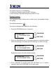
NT 250 Technical and Maintenance Manual NicomUsa Inc RUNNING THE PROGRAM Once the program is running, from the main screen it is necessary to click the POWER ON button; the screen will light up and a message" COMMUNICATION IN PROGRESS" will appear. After few seconds, on the left side of the screen, the operating frequency will appear together with all the other parameters. If not, check the Communication port setting (COM1-COM 2). To change it, click the File menu and then select "set Port".
NT 250 PROGRAMMING Connect a 50 ohm load or 50 ohm antenna to the RF output, connect the equipment into a mains supply (100÷240 VAC). The equipment is factory pre-set to 50 W. Switch ON the power and the yellow V POWER LED will light. The Display will show: PROGRAM WAIT SETTING After 3 seconds the green PLL LOCK led will light and the Display will show an increasing bar. After a further 5 seconds the green ENABLE will light and there will be output power.
The default frequency is 98.000 MHz. To display the frequency push the SETTING key. In order to display the parameter push the SELECT key. Display Password The Password mode is factory set to enable, and is not possible change this setting. The default password is 1 2 3.
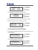
CONFIRM (Y/N) ? N=SEL. Y=SET. PROGRAM SETTING If the password is not correct an error is displayed: ERROR PASSWORD PROGRAM SETTING After a few seconds the display will show the parameters again. • When the password is correct, the display will show: NEW PASS . = SET. NEW FREQ . = PRG PROGRAM SETTING To change the password press the SETTING key. To change the frequency press the PROGRAM key.
If the password is correct the display will show: STORED NEW PASSWORD PROGRAM SETTING If the confirmation password is wrong the display will show: ERROR CONFIRMATION PROGRAM SETTING IMPORTANT NOTE ! BE CAREFUL ! Once the password is set, it must be remembered, otherwise neither the frequency nor the password can be reset and the unit will have to be returned to Nicom for resetting. Display Change of Frequency. • Press the PROGRAM key for 3 seconds and enter the correct password.
The underscore character indicates which digit can be change. To move the underscore character hit the PROGRAM key. When the new frequency is chosen, then press the SETTING key confirm it. After a “WAIT CYCLE”, the display will show the parameters: MOD > FRW 50W RFL 0.4W PROGRAM SETTING After 7 minutes the display light will switch off and the display will show: NICOM MHz 103.
NT 250 Technical and Maintenance Manual NicomUsa Inc CHAPTER 2 ELECTRICAL SPECIFICATIONS NT 250 TECHNICAL DATA Power output: Frequency of operation: RF output connector/ Impedance: Frequency Stability: Frequency Range: 2 to 270 Watts continuously variable Sinthesized with TXCO crystal reference Type "N" Female / 50 Ohms Better than 5ppm (± 500 Hz) , 0 to 50° C. 87.5 - 108 Mhz Frequency programming: Modulation type: S/N Ratio (ref.
NT 250 Technical and Maintenance Manual COMPOSITE OPERATION Composite inputs MPX input MPX input impedance MPX input level Composite FM unweighed S/N ratio Composite Total Harmonic Distortion Composite Intermodulation Distortion Baseband Crosstalk SCA Inputs SCA Input Impedance SCA Input Levels SCA Amplitude Response Crosstalk NicomUsa Inc four total, 1 for MPX and 3 for SCA 1 unbalanced bnc connector 2 K ohms 3,5 V p-p (1,237 Vrms/3.
NT 250 Technical and Maintenance Manual NicomUsa Inc MECHANICAL SPECIFICATIONS Chassis Dimensions: 132 mm (5.1") H 326 mm (12.83")D 445 mm (17.51) W Front panel dimensions: 483 mm (19") W 132 mm (5.1") H Ambient operating temperature: from 0 to + 50 C (+32 to +122 F) Humidity: 90% maximum, non condensing. Weight: 32 Lbs ( 14.
LOCK ENABLE PROGRAM 3 4 5 6 7 PWR ADJ.
3 RF OUTPUT 50 OHM 250W REMOTE CONTROL 6 7 8 1 GND 2+ 3- 9 10 11 13 SCA 3 SCA 2 SCA 1 MONO 50 75 S MPX 14 4 16 12 15 INTERLOCK 5 WARNING Voltages under equipment cover plate can be hazardous to your life. Equipment only can be handled by qualified personnel. FU SE MAINS V A 1 2 1 - MAIN SUPPLY CONNECTOR 2 - AC FUSE 3A 3 - FAN 4 - DB 9 PIN INPUT / OUTPUT CONNECTOR FOR TELEMETRY ( opt.
RF DRIVER RF AMPLIFIER LIMITER LPF DIRECTIONAL COUPLER VCO RF OUTPUT MPX ADJ MONO AUDIO INPUT PLL SIGNAL INTERFACE SCA TCXO 12.8 MHz RS232 DISPLAY VAC POWER SUPPLY VDC MICROCONTROLLER NICOM MHz 98.000 Title N COM FUNCTIONAL SCHEMATIC Size B Date: Document Number Rev 1.0 Mod.
J5 BNC GND J6 BNC + C TX L7 CHOKE L6 CHOKE L5 CHOKE L4 CHOKE L3 CHOKE L2 CHOKE L1 CHOKE 2 F2 150mA L N 1 RX 5 9 4 8 3 7 2 6 1 P1 DB9 MALE COAX1 RG303 RF FILTER 2 J4 BNC FAN2 12 V J1 RF OUTPUT 1 J3 BNC RS232 SCA3 INTERLOCK SCA2 JR1 XLR J2 BNC F1 3.
TERM4 FUSE A TERM5 FUSE B L8 0.8mH TERM1 TERM6 L IN L OUT C1 2.2nF / 350V TERM2 GND HEART RV1 275V C2 1uF / 350V RV2 275V C3 2.2nF / 350V TERM3 SW1 RV3 275V L9 0.8mH TERM7 N IN N OUT Title N COM EMC FILTER Size A Date: Document Number Rev 1.0 Mod.
+24V R1 1K LED PW J2 SMB V-ADJ VADJ IN FWD PW FORWARD POWER IN RFL PW REFLECT POWER -15V LED RF LED RF INTERLOCK 2 DRIVER OFF VC 1 SCA 2 VD 2 -15V VA TEMP.
STEREO C26 60pF VA R5 27K 8 U1B OP275 R6 47K + 7 - U1A OP275 R8 47K 5 6 R7 12K + 1 R9 5K J14 DJ3 2 4 MODULATION BF OUT 3 LIMITER VB R10 27K GND BF OUT R11 47K D3 BAT43 R15 1K2 D4 BAT43 R17 3K9 R16 200 R12 1K GND SCA 1 +15V C28 22pF -15V R18 1K2 SCA 1 C29 470pF R14 12K C27 10pF R19 3K9 SCA 2 C31 1000MF / 35V + R13 10K C32 470pF R21 12K R20 1K GND SCA 2 + C30 100MF / 16V SCA 3 C33 470pF R23 12K +15V R22 1K GND SCA 3 R24 33 R25 220K R179 20K + C34 10MF / 35V MPX
LCD1 DISPLAY V20350 +5V +5V +5V +5V JP1 Y1 11.0592MHz V0 _V0 VCC _VCC GND _GND LED _LEDLED + _LED+ NC _NC 3 20 2 19 1 18 15 32 16 33 17 34 4 21 5 22 6 23 DB0 _DB0 DB1 _DB1 DB2 _DB2 DB3 _DB3 DB4 _DB4 DB5 _DB5 DB6 _DB6 DB7 _DB7 D7 3 +5V D[0:7] RST 1 C50 22MF / 16V + RS C52 0.
+15V D10 LED R73 1K2 L12 N.C. U8 N.C. C66 0.1MF C61 100MF / 35V + 2 1 FB ON/OFF C67 0.1MF D12 N.C. + C62 1000MF / 25V C63 100MF / 25V + C64 47MF / 16V + UA7805 IN C68 0.1MF +5V 3 OUT GND + U9 OUTPUT C69 0.1MF C65 47MF / 16V + D11 LED 3 C60 1000MF / 35V 4 5 V IN 2 1 GND +24V L13 22uH R74 390 GND R75 33 VA C71 0.1MF + C70 22MF / 16V C72 0.1MF + C73 22MF / 16V C75 0.
+24V +24V +15V +15V +5V +5V +5V +15V C91 10MF / 35V +24V + R81 47K U12A LM358 8 R83 100K R85 47K 3 + 2 R82 47K D16 5V1 R84 47K Q2 BC327 1 - R87 2K2 LED RF -15V R86 47K 4 GND R88 150 -15V R89 150 R90 33 ADJ-A C92 0.1MF + C93 470MF / 35V + C94 470MF / 35V Rext 2 5K ADJ-B R91 10 RF ADJ. ADJ-C D17 LL4148 +5V R92 4K7 Q3 BC337 D18 LL4148 R93 47K R94 47K DRIVER OFF R95 47K +24V Interlock Q4 BC327 R96 12K C95 0.1MF Q5 BC337 Q6 TIP41 R97 47K + + C97 2.
R120 22 R121 47 +15V R122 22 U15 UA7808 C106 1000MF / 16V + C107 2.2MF / 50V OUT 3 + C108 2.2MF / 50V C110 0.1MF + C109 1000MF / 16V 2 + IN GND R123 47 1 GND R124 82 C112 0.1MF + R125 82 C111 10MF / 35V C113 0.1MF R126 680 R127 680 COAX1 RG178 Q8 J310 D20 MV209 D21 MV209 D22 MV209 D23 MV209 C116 100pF + Q9 J310 D25 MV209 D26 MV209 D27 MV209 R128 330 4 C117 3.3pF D24 MV209 C114 10MF / 35V C115 0.1MF L16 2.2µH 1 U16 ERA6 3 2 V-VCO R129 10 C118 2.
+5V GND C126 0.1MF + C124 10MF / 35V + C125 22MF / 16V TCXO1 MHz 12.800 C127 0.1MF 1 N.C Vcc GND OUT 14 +15V R135 56K 7 Q10 BC327 R137 100 R138 18K + C129 1nF R139 330 R142 100 U18A LM358 V-VCO 1 R145 120K + 1 C131 100MF / 35V 2 + 3 - 2 3 4 R143 560 4 R144 1K R140 4K7 8 R141 10K C130 2.2MF / 50V R136 10K C128 22MF / 16V D28 LL4148 + + R146 3K9 C133 0.
ADJ-POWER +15V C141 0.1MF GND + C142 10MF / 35V R162 22K D32 LL4148 R163 10 R164 10 DRIVER OFF R166 18K R165 10K C143 0.1MF R167 470 L20 18T/0.4D C146 0.1MF R170 330 R171 330 + C145 1nF C144 10MF / 35V C153 0.1MF RF INPUT GND RF INPUT R178 56 Q13 BFR96 C151 1nF C154 39pF L23 2T/.6D C155 NC C156 NC C147 4.7nF R173 39 R175 470 R177 12K R168 R169 12 390 R172 10 R174 10 R176 12 L24 3T/.6D L21 3T/.6D L22 3T/.
NICOM Rif. C103 C104 C105 C106 C107 C108 C109 C110 C111 C112 C113 C114 C115 C116 C117 C118 C119 C120 C121 C122 C123 C124 C125 C126 C127 C128 C129 C130 C131 C132 C133 C134 C135 C136 C137 C138 C139 C140 C141 C142 C143 C144 C145 C146 C147 C148 C149 C150 C151 C152 C153 C154 C155 Value 2.2MF / 50V 10MF / 35V 0.1MF 1000MF / 16V 2.2MF / 50V 2.2MF / 50V 1000MF / 16V 0.1MF 10MF / 35V 0.1MF 0.1MF 10MF / 35V 0.1MF 100pF 3.3pF 2.2MF / 50V 3.3pF 100pF 47MF / 16V 100pF 22pF 10MF / 35V 22MF / 16V 0.1MF 0.
NICOM Rif. Value Remarks C156 C157 C158 C159 C160 NC 22pF 22pF 0.1MF 1nF L1 L2 L3 L4 L5 L6 L7 L8 L9 L10 L11 L12 L13 L14 L15 L16 L17 L18 L19 L20 L21 L22 L23 L24 22uH 22uH 22uH 22uH 22uH 22uH 22uH 22uH 22uH 22uH 22uH 22uH 150uH 22uH 2.2µH 22µH 8T/0.6D 22µH 18T/0.4D 3T/.6D 3T/.6D 2T/.6D 3T/.
NICOM Rif.
NICOM Rif.
NICOM Rif.
NICOM Rif.
NICOM Rif. Value U1 U2 U3 U4 U5 U6 U7 U8 U9 U10 U11 U12 U13 U14 U15 U16 U17 U18 OP275 LM358 LF353 ADC0834 MAX810L T89C51RD2 MAX232 MC78M05CDT LM2575/S15 MC79M05CDT LM358 LM358 LM358 MC78M08CDT ERA6 LMX1501 LM358 Y1 TCXO1 11.0592MHz MHz 12.800 LCD1 SW1 FILT1 COAX1 DISPLAY DB9 MONITOR FILTER 19KHz RG178 J1 J2 J3 J4 J5 J6 J7 J8 J9 J10 J11 J12 J13 J14 J15 J16 J17 J18 J19 J20 POWER SMB DJ2x5 NC STEREO NC DJ3 NC NC NC NC DB9_AUX DB9 DJ3 DJ3 DJ2 DJ2 TEST Fref.
R4 0 1 R2 0 R5 0 2 R7 ADJ-FM/ADJ-TX R18 0 R8 0 3 D1 +15V R10 0-FM D2 +24V J2 RJ45 D4 ENABLE 1 2 3 4 5 6 7 8 R6 0 D5 LOCK PLL R23 0 R20 0-FM R22 0-FM Title N COM Frontal Panel Size A Date: Document Number Rev 1.0 Mod.
NICOM Part List Schematic : MIFP01 Rif. Value Remarks C1 C2 C3 C4 C5 R1 R2 R3 R4 R5 R6 R7 R8 R9 R10 R11 R12 R13 R14 R15 R16 R17 R18 R19 R20 R21 R22 R23 R24 D1 D2 D3 D4 D5 D6 N.C. N.C. N.C. N.C. N.C. 0 1/4W 0 0 0 5K 0 1/4W 1/4W 1/4W 1/4W 1/4W 0 1/4W 0 1/4W 0 1/4W 0 0 1/4W 1/4W +15V +24V ENABLE LOCK PLL SW1 U1 J1 J2 Description N.C. Carbon Film Resistor N.C.
RF MODULE 250W J1 BNC RF FILTER & Power Meter RF INPUT RF INPUT +48V +48V TERM2 COAX1 RG303 L1 0.5T / 1.5D TERM1 RF OUTPUT RF INPUT J2 N RF OUTPUT RF OUPUT C1 1nF GATES GATE C2 1nF SCHEMATIC3 L2 4.7uH TERM3 TEMPERATURE C3 1nF C4 10nF C5 100nF D1 LM335 Title N COM RF AMPLIFIER 250W Size B Date: Document Number Rev 1.0 Mod.
+48V + R1 3K3 / 3W C6 100MF / 63V + C7 10MF / 100V + C8 10MF / 100V C9 1nF C10 100pF R2 10K C11 100nF C12 10nF D2 5V1 R3 2K2 R4 10K L3 RF-CHOKE L4 4.7uH D3 1N4148 R5 100 R6 6K8 GATE C14 10nF C15 100nF + C13 4.7MF / 63V C16 10nF R7 100K D4 1N4148 C17 10nF C18 470pF R8 10 R9 10 TR1 TR2 C20 100pF L5 3T / 1D C19 470pF RF OUTPUT RF INPUT TR3 C22 10pF Q1 SD2932 C25 33pF R10 10 / 1W C21 4.7nF C23 470pF L6 0.5T / 1.5D TR4 C24 2.2nF C26 4.7nF C27 4.
C31 10pF C32 10pF C33 22pF C34 10pF C35 22pF Power Meter L7 2T/1.5mm L8 4T/1.5mm L9 4T/1.5mm L10 4T/1.5mm RF INPUT RF IN C36 10pF C37 39pF C38 27pF C39 27pF C40 27pF C41 27pF C42 27pF RF OUPUT RF OUT C43 6.8pF C44 6.8pF Title N COM RF Filter + Power Meter Size A3 Date: Document Number Rev 1.0 Mod.
CT1 RF IN RF OUT C45 1.8pF C46 1.8pF L11 4.7uH R13 1K C47 22pF R14 150 / 3W R15 150 / 3W D5 BAT43 R16 15K R17 1K2 C52 22pF D6 BAT43 R18 1K2 Forward Power Reflected Power R19 6K8 C48 10nF C49 1nF C50 1nF C51 10nF Title N COM Forward and Reflected Power Meter Size A Date: Document Number Rev 1.0 Mod.
NICOM Part List Schematic : RFAMP250W Rif. C1 C2 C3 C4 C5 C6 C7 C8 C9 C10 C11 C12 C13 C14 C15 C16 C17 C18 C19 C20 C21 C22 C23 C24 C25 C26 C27 C28 C29 C30 C31 C32 C33 C34 C35 C36 C37 C38 C39 C40 C41 C42 C43 C44 C45 C46 C47 C48 C49 Value 1nF 1nF 1nF 10nF 100nF 100MF 10MF 10MF 1nF 100pF 100nF 10nF 4.7MF 10nF 100nF 10nF 10nF 470pF 470pF 100pF 4.7nF 10pF 470pF 2.2nF 33pF 4.7nF 4.7nF 470pF 470pF 10nF 10pF 10pF 22pF 10pF 22pF 10pF 39pF 27pF 27pF 27pF 27pF 27pF 6.8pF 6.8pF 1.8pF 1.
NICOM Rif. Value C50 C51 C52 1nF 10nF 22pF L1 L2 L3 L4 L5 L6 L7 L8 L9 L10 L11 0.5T / 1.5D 4.7uH RF-CHOKE 4.7uH 3T / 1D 0.5T / 1.5D 2T/1.5mm 4T/1.5mm 4T/1.5mm 4T/1.5mm 4.
NICOM Rif.