PR533 USB NFC integrated reader solution Rev. 3.6 — 27 October 2014 206436 Product short data sheet COMPANY PUBLIC 1. General description The PR5331C3HN is a highly integrated transceiver module for contactless reader/writer communication at 13.56 MHz. A dedicated ROM code is implemented to handle different RF protocols by an integrated microcontroller. The system host controller communicates with the PR5331C3HN by using the USB or the HSU link.
PR533 NXP Semiconductors USB NFC integrated reader solution Support of USB 2.0 full speed, interoperable with USB 3.0 hubs. The PR533C3HN in PCD mode is compliant with EMV contactless specification V2.0.1. 1.
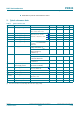
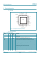
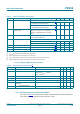
PR533 NXP Semiconductors USB NFC integrated reader solution Dedicated I/O ports for external device control 3. Quick reference data Table 1. Quick reference data Symbol Parameter VBUS bus supply voltage Conditions Min Typ Max Unit 4.02 5 5.25 V 2.5 3.3 3.6 V [1] 2.5 3.3 3.6 V [1] 2.5 3.3 3.
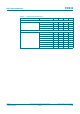
PR533 NXP Semiconductors USB NFC integrated reader solution 4. Ordering information Table 2. Ordering information Type number Package Name PR5331C3HN/C360[1][2][3] PR5331C3HN/C370[1][2][3] Description Version HVQFN40 plastic thermal enhanced very thin quad flat package; no leads; 40 terminals; body 6 6 0.85 mm SOT618-1 [1] 60 or 70 refers to the ROM code version described in the User Manual. For differences of romcode versions refer to the release note of the product.
PR533 NXP Semiconductors USB NFC integrated reader solution 6. Pinning information 31 P33_INT1 32 P50_SCL 33 SDA 34 P34 35 SIGOUT 36 SIGIN 37 SVDD 38 RSTPD_N terminal 1 index area 39 DVDD 40 VBUS 6.
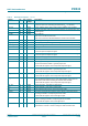
PR533 NXP Semiconductors USB NFC integrated reader solution Table 3. PR533 pin description …continued Symbol Pin Type Pad ref voltage Description OSCIN 15 I AVDD crystal oscillator input: input to the inverting amplifier of the oscillator. This pin is also the input for an externally generated clock (fclk = 27.12 MHz). OSCOUT 16 O AVDD crystal oscillator output: output of the inverting amplifier of the oscillator.
PR533 NXP Semiconductors USB NFC integrated reader solution Table 3. PR533 pin description …continued Symbol Pin Type Pad ref voltage Description RSTPD_N 38 I reset and power-down: When LOW, internal current sources are switched off, the oscillator is inhibited, and the input pads are disconnected from the outside world. PVDD With a negative edge on this pin the internal reset phase starts. DVDD 39 P digital power supply VBUS 40 P USB power supply.
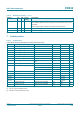
PR533 NXP Semiconductors USB NFC integrated reader solution 8. Recommended operating conditions Table 5. Operating conditions Symbol Parameter Conditions Min Typ Max Unit VBUS bus supply voltage VSSA = VSSD = VSS(PVSS) = VSS(TVSS) = 0 V 4.02 5 5.25 V supply voltage (non-USB mode); VBUS = VDDD; VSSA = VSSD = VSS(PVSS) = VSS(TVSS) = 0 V 2.5 3.3 3.6 V VDDA analog supply voltage VDDA = VDDD = VDD(TVDD) = VDD(PVDD); VSSA = VSSD = VSS(PVSS) = VSS(TVSS) = 0 V [1][2] 2.5 3.3 3.
PR533 NXP Semiconductors USB NFC integrated reader solution Table 7. Current consumption characteristics Symbol Parameter Conditions Min Ipd power-down current VDDA = VDDD = VDD(TVDD) = VDD(PVDD) = 3 V; not powered from USB - 1.
PR533 NXP Semiconductors USB NFC integrated reader solution Table 9.
PR533 NXP Semiconductors USB NFC integrated reader solution 10.3 Typical 27.12 MHz Crystal requirements Table 10. Crystal requirements Symbol Parameter Conditions Min Typ Max Unit fxtal crystal frequency 27.107 27.12 27.133 MHz ESR equivalent series resistance - - 100 CL load capacitance - 10 - pF Pxtal crystal power dissipation 100 - - W 10.4 Pin characteristics for 27.12 MHz XTAL Oscillator (OSCIN, OSCOUT) Table 11. Pin characteristics for 27.
PR533 NXP Semiconductors USB NFC integrated reader solution 10.5 RSTPD_N input pin characteristics Table 12. RSTPD_N input pin characteristics Symbol Parameter Conditions Min Typ Max Unit VIH HIGH-level input voltage VDD(PVDD) 0.4 - VDD(PVDD) V VIL LOW-level input voltage 0 - 0.4 V IIH HIGH-level input current 1 - 1 A IIL LOW-level input current VI = 0 V 1 - 1 A Ci input capacitance - 2.5 - pF VI = VDD(PVDD) 10.
PR533 NXP Semiconductors USB NFC integrated reader solution 10.7 RSTOUT_N output pin characteristics Table 14. RSTOUT_N output pin characteristics Symbol Parameter VOH VOL IOH Conditions Max Unit 0.7 VDD(PVDD) - VDD(PVDD) V 0.7 VDD(PVDD) - VDD(PVDD) V VDD(PVDD) = 3 V; IOH = 4 mA LOW-level output voltage VDD(PVDD) = 3 V; IOL = 4 mA 0 - 0.3 VDD(PVDD) V VDD(PVDD) = 1.8 V; IOL = 2 mA [1] 0 - 0.3 VDD(PVDD) V HIGH-level output current VDD(PVDD) = 3 V; VOH = 0.
PR533 NXP Semiconductors USB NFC integrated reader solution 10.8 Input/output characteristics for pin P70_IRQ Table 15. Input/output pin characteristics for pin P70_IRQ Symbol Parameter Conditions VIH HIGH-level input voltage [1] VIL LOW-level input voltage [2] VOH HIGH-level output voltage push-pull mode; VDD(PVDD) = 3 V; IOH = 4 mA push-pull mode; VDD(PVDD) = 1.8 V; IOH = -2 mA VOL LOW-level output voltage [3] push-pull mode; VDD(PVDD) = 3 V; IOL = 4 mA push-pull mode; VDD(PVDD) = 1.
PR533 NXP Semiconductors USB NFC integrated reader solution 10.9 Input/output pin characteristics for P30 / UART_RX, P31 / UART_TX, P32_INT0, P33_INT1 Table 16. Input/output pin characteristics for P30 / UART_RX, P31 / UART_TX, P32_INT0, P33_INT1 Symbol Parameter Conditions Min VIH HIGH-level input voltage [1] VIL LOW-level input voltage [2] VOH HIGH-level output voltage push-pull mode; VDD(PVDD) = 3 V; IOH = 4 mA VDD(PVDD) = 1.
PR533 NXP Semiconductors USB NFC integrated reader solution 10.10 Input/output pin characteristics for P35 Table 17. Input/output pin characteristics for P35 Symbol Parameter Min Typ Max Unit HIGH-level input voltage [1] 0.7 VDDD - VDDD V VIL LOW-level input voltage [2] 0 - 0.3 VDDD V VOH HIGH-level output voltage VDDD 0.4 - VDDD V VOL LOW-level output voltage VDDD = 3 V; IOL = 4 mA 0 - 0.
PR533 NXP Semiconductors USB NFC integrated reader solution 10.11 Input/output pin characteristics for DP and DM Table 18. Input/output pin characteristics for DP and DM for USB interface Symbol Parameter Conditions HIGH-level input voltage VIH VDD(PVDD) = 3.3 V [1] Min Typ Max Unit 2 - 3.6 V 0 - 0.8 V VIL LOW-level input voltage VOH HIGH-level output voltage VDD(PVDD) = 3.3 V; RPD = 1.5 to VSS 2.8 - VDD(PVDD) V VOL LOW-level output voltage VDD(PVDD) = 3.3 V; RPD = 1.
PR533 NXP Semiconductors USB NFC integrated reader solution Table 19. USB DP/DM differential receiver input levels Symbol Parameter Conditions Min Typ Max Unit VDI differential input sensitivity voltage - 0.2 - - V VCM differential common mode voltage range - 0.8 - 2.5 V Table 20.
PR533 NXP Semiconductors USB NFC integrated reader solution Table 21. Input Pin characteristics for DP for HSU interface Symbol Parameter Min Typ Max Unit HIGH-level input voltage [1] 0.7 VDD(PVDD) - VDD(PVDD) V VIL LOW-level input voltage [2] 0 - 0.3 VDD(PVDD) V IIH HIGH-level input current Vi = VDD(PVDD) - - 1 mA IIL LOW-level input current Vi = 0 V - - 1 mA ILI input leakage current RSTPD_N = 0 V 1 1 mA Ci input capacitance 3.5 pF VIH Conditions - 2.
PR533 NXP Semiconductors USB NFC integrated reader solution 10.12 Input pin characteristics for SCL Table 23. Input/output drain output pin characteristics for SCL I2C interface Symbol Parameter Conditions Min Max Unit 0.7 VDD(PVDD) - VDDD V 0 - 0.3 VDDD V VDDD = 3 V; IOL = 4 mA 0 - 0.3 V HIGH-level input current VI = VDDD 1 - 1 A IIL LOW-level input current VI = 0 V 1 - 1 A RSTPD_N = 0.4 V 1 - 1 A - 2.
PR533 NXP Semiconductors USB NFC integrated reader solution 10.14 Output pin characteristics for DELATT Table 25. Output pin characteristics for DELATT Symbol Parameter VOH HIGH-level output voltage VIL LOW-level input voltage Conditions [1] Min Typ Max Unit 0.7 VDD(SVDD) - VDD(SVDD) V 0 - 0.3 VDD(PVDD) V IIH HIGH-level input current input mode; VI = VDD(SVDD) 1 - 1 A IIL LOW-level input current input mode; VI = 0 V 1 - 1 A ILI input leakage current RSTPD_N = 0.
PR533 NXP Semiconductors USB NFC integrated reader solution 10.17 Input/output pin characteristics for P34 Table 28. Input/output pin characteristics for P34 Symbol Parameter Conditions Min Typ Max Unit 0.7 VDD(SVDD) - VDD(SVDD) V 0 0.3 VDD(SVDD) V HIGH-level input voltage [1] VIL LOW-level input voltage [2] VOH HIGH-level output voltage push-pull; VDDD 0.1 < VDD(SVDD) < VDDD IOH = 4 mA VDD(SVDD) 0.4 - VDD(SVDD) V VOL LOW-level output voltage push-pull; VDDD 0.
PR533 NXP Semiconductors USB NFC integrated reader solution 10.19 Input pin characteristics for RX Miller coded signals Vin, RX AVDD +1 V mRXmil = VRX, IV, mil - Vmod VRX, IV, mil + Vmod VRX, IV, mil Vmod VMID 13.56 MHz carrier 0V Manchester coded signals Vin, RX AVDD +1 V VRXMod, Man VRX, IV, Man Vmod VMID 13.56 MHz carrier 0V aaa-002342 Fig 5. Table 30.
PR533 NXP Semiconductors USB NFC integrated reader solution Table 30.
PR533 NXP Semiconductors USB NFC integrated reader solution 10.21 Output pin characteristics for TX1/TX2 Table 32. Output pin characteristics for TX1/TX2 Symbol Parameter Conditions Min Typ Max Unit VOH HIGH-level output voltage VDD(TVDD) = 3 V; IO = 32 mA; CWGsN = Fh - - 150 mV VDD(TVDD) = 3 V; IO = 80 mA; CWGsN = Fh - - 400 mV VDD(TVDD) = 2.5 V; IO = 32 mA; CWGsN = Fh - - 240 mV VDD(TVDD) = 2.5 V; IO = 80 mA; CWGsN = Fh - - 640 mV Typ Max Unit VOL Table 33.
PR533 NXP Semiconductors USB NFC integrated reader solution 10.22 System reset timing Vth(rst)reg + Vth(rst)reg(hys) VDD(PVDD) Vth(rst)reg(hys) RSTPD_N trst tw(rst) tPOR RSTOUT_N 001aao394 Fig 6. System reset overview Table 34. Reset duration time Symbol Parameter tPOR trst tw(rst) Min Typ Max Unit power-on reset time [1] 0.1 0.4 2 ms reset time hard power-down time; user dependent [2] 20 - - ns reset time when RSTPD_N is released [1] 0.1 0.
PR533 NXP Semiconductors USB NFC integrated reader solution 10.23 Timing for the I2C-bus interface SDA tSU;DAT tf tSP tr tHD;STA tf tLOW tBUF SCL tr tHD;STA S tHIGH tSU;STA tHD;DAT tSU;STO Sr P S 001aaj635 Fig 7. Table 35.
PR533 NXP Semiconductors USB NFC integrated reader solution 10.24 Temperature sensor Table 36. Symbol Tth(act)otp [1] PR533_SDS Product short data sheet COMPANY PUBLIC Temperature sensor characteristics Parameter Conditions overtemperature protection activation threshold temperature CIU [1] Min Typ Max Unit 100 125 140 C The temperature sensor embedded in the PR533 is not intended to monitor the temperature. Its purpose is to prevent destruction of the IC due to excessive heat.
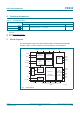
PR533 NXP Semiconductors USB NFC integrated reader solution 11. Application information interface supply SVDD RSDA SIGOUT RSCL SDA SECURE CORE SIGIN l 2C MEMORY P50_SCL P34 CRX RX supply R1 R2 VMID VBUS CVMID DVDD antenna PR533 PVDD HOST - PROCESSOR TX1 C0 TVSS1 TVSS2 RTSPD_N C1 L0 C0 host interface TX2 P70_IRQ L0 RQ C2 C1 C2 RQ TVDD AVDD DVSS AVSS OSCIN OSCOUT 27.12 MHz aaa-000042 Fig 8. Application diagram of PR533 12. Abbreviations Table 37.
PR533 NXP Semiconductors USB NFC integrated reader solution 13. Revision history Table 38. Revision history Document ID Release date Data sheet status Change notice Supersedes PR533_SDS v.3.6 20141027 Product short data sheet - PR533_SDS v.3.5 - PR533_SDS v.3.4 - PR533_SDS v.3.2 - PR5331C3HN_SDS v.3.0 - - Modifications: PR533_SDS v.3.5[1] Modifications: PR533_SDS v.3.3 Modifications: PR533_SDS v.3.2 Modifications: • Section 1.
PR533 NXP Semiconductors USB NFC integrated reader solution 14. Legal information 14.1 Data sheet status Document status[1][2] Product status[3] Definition Objective [short] data sheet Development This document contains data from the objective specification for product development. Preliminary [short] data sheet Qualification This document contains data from the preliminary specification. Product [short] data sheet Production This document contains the product specification.
PR533 NXP Semiconductors USB NFC integrated reader solution Export control — This document as well as the item(s) described herein may be subject to export control regulations. Export might require a prior authorization from competent authorities. Quick reference data — The Quick reference data is an extract of the product data given in the Limiting values and Characteristics sections of this document, and as such is not complete, exhaustive or legally binding.
PR533 NXP Semiconductors USB NFC integrated reader solution Notes PR533_SDS Product short data sheet COMPANY PUBLIC All information provided in this document is subject to legal disclaimers. Rev. 3.6 — 27 October 2014 206436 © NXP Semiconductors N.V. 2014. All rights reserved.
PR533 NXP Semiconductors USB NFC integrated reader solution 16. Tables Table 1. Table 2. Table 3. Table 4. Table 5. Table 6. Table 7. Table 8. Table 9. Table 10. Table 11. Table 12. Table 13. Table 14. Table 15. Table 16. Table 17. Table 18. Table 19. Table 20. Table 21. Table 22. Table 23. Table 24. Table 25. Table 26. Table 27. Table 28. Table 29. Table 30. Table 31. Table 32. Table 33. Table 34. Table 35. Table 36. Table 37. Table 38. Quick reference data . . . . . . . . . . . . . . . . . . . . .
PR533 NXP Semiconductors USB NFC integrated reader solution 17. Figures Fig 1. Fig 2. Fig 3. Fig 4. Fig 5. Fig 6. Fig 7. Fig 8. Block diagram . . . . . . . . . . . . . . . . . . . . . . . . . . . .4 Pin configuration for HVQFN 40 (SOT618-1) . . . .5 27.12 MHz input clock phase noise spectrum mask . . . . . . . . . . . . . . . . . . . . . . . . . . . . . . . . . . 11 Transmit waveform at DP/DM . . . . . . . . . . . . . . .18 RX input parameters . . . . . . . . . . . . . . . . . . . . . .
PR533 NXP Semiconductors USB NFC integrated reader solution 18. Contents 1 1.1 1.2 1.3 1.4 2 3 4 5 6 6.1 6.2 7 8 9 10 10.1 10.1.1 10.1.2 10.2 10.3 10.4 10.5 10.6 10.7 10.8 10.9 10.10 10.11 10.12 10.13 10.14 10.15 10.16 10.17 10.18 10.19 10.20 10.21 10.22 10.23 10.24 General description . . . . . . . . . . . . . . . . . . . . . . 1 RF protocols . . . . . . . . . . . . . . . . . . . . . . . . . . . 1 Interfaces . . . . . . . . . . . . . . . . . . . . . . . . . . . . . 1 Standards compliancy. . . . . . .