
User's Manual
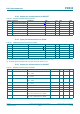
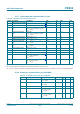
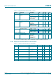
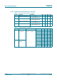
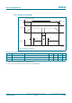
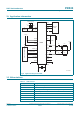
Table Of Contents
- 1. General description
- 2. Features and benefits
- 3. Quick reference data
- 4. Ordering information
- 5. Block diagram
- 6. Pinning information
- 7. Limiting values
- 8. Recommended operating conditions
- 9. Thermal characteristics
- 10. Characteristics
- 10.1 Power management characteristics
- 10.2 Antenna presence self test thresholds
- 10.3 Typical 27.12 MHz Crystal requirements
- 10.4 Pin characteristics for 27.12 MHz XTAL Oscillator (OSCIN, OSCOUT)
- 10.5 RSTPD_N input pin characteristics
- 10.6 Input pin characteristics for I0, I1 and TESTEN
- 10.7 RSTOUT_N output pin characteristics
- 10.8 Input/output characteristics for pin P70_IRQ
- 10.9 Input/output pin characteristics for P30 / UART_RX, P31 / UART_TX, P32_INT0, P33_INT1
- 10.10 Input/output pin characteristics for P35
- 10.11 Input/output pin characteristics for DP and DM
- 10.12 Input pin characteristics for SCL
- 10.13 Input/output pin characteristics for SDA
- 10.14 Output pin characteristics for DELATT
- 10.15 Input pin characteristics for SIGIN
- 10.16 Output pin characteristics for SIGOUT
- 10.17 Input/output pin characteristics for P34
- 10.18 Output pin characteristics for LOADMOD
- 10.19 Input pin characteristics for RX
- 10.20 Output pin characteristics for AUX1/AUX2
- 10.21 Output pin characteristics for TX1/TX2
- 10.22 System reset timing
- 10.23 Timing for the I2C-bus interface
- 10.24 Temperature sensor
- 11. Application information
- 12. Abbreviations
- 13. Revision history
- 14. Legal information
- 15. Contact information
- 16. Tables
- 17. Figures
- 18. Contents
PR533_SDS All information provided in this document is subject to legal disclaimers. © NXP Semiconductors N.V. 2014. All rights reserved.
Product short data sheet
COMPANY PUBLIC
Rev. 3.6 — 27 October 2014
206436 24 of 36
NXP Semiconductors
PR533
USB NFC integrated reader solution
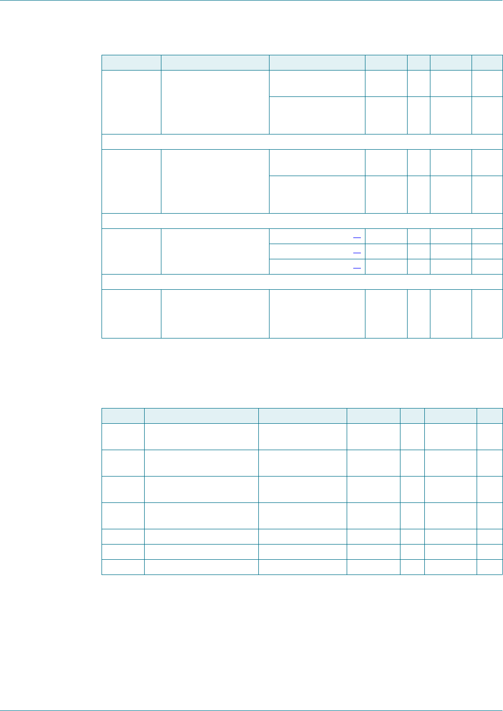
[1] The minimum modulation voltage is valid for all modulation schemes except Miller coded signals.
10.20 Output pin characteristics for AUX1/AUX2
V
RX(p-p)
peak-to-peak receiver
voltage
Miller coded;
106 kbit/s
-150500mV
Manchester
coded; 212 kbit/s
and 424 kbit/s
-100200mV
Maximum dynamic input voltage
V
RX(p-p)
peak-to-peak receiver
voltage
Miller coded;
106 kbit/s
V
DDA
-- V
Manchester
coded;
212 and 424 kbit/s
V
DDA
-- V
Minimum modulation voltage
V
mod
modulation voltage RxGain = 6 and 7
[1]
--6mV
RxGain = 4 and 5
[1]
--18mV
RxGain = 0 to 3
[1]
--120mV
Minimum modulation index
m modulation index Miller coded;
106 kbit/s
V
RX(p-p)
=1.5V;
SensMiller = 3
-33-%
Table 30. Input pin characteristics for RX …continued
Symbol Parameter Conditions Min Typ Max Unit
Table 31. Output pin characteristics for AUX1/AUX2
Symbol Parameter Conditions Min Typ Max Unit
V
OH
HIGH-level output voltage V
DDD
=3V;
I
OH
= 4mA
V
DDD
0.4 - V
DDD
V
V
OL
LOW-level output voltage V
DDD
=3V;
I
OL
=4mA
V
SSD
-V
SSD
+0.4 V
I
OH
HIGH-level output current V
DDD
= 3 V; V
OH
=
V
DDD
0.3
4-- mA
I
OL
LOW-level output current V
DDD
= 3 V; V
OL
=
V
DDD
-0.3
4--mA
I
LI
input leakage current RSTPD_N = 0 V 1-+1A
C
i
input capacitance - 2.5 - pF
C
L
load capacitance - - 15 pF