
User's Manual
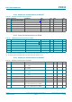
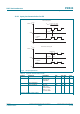
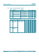
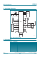
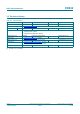
Table Of Contents
- 1. General description
- 2. Features and benefits
- 3. Quick reference data
- 4. Ordering information
- 5. Block diagram
- 6. Pinning information
- 7. Limiting values
- 8. Recommended operating conditions
- 9. Thermal characteristics
- 10. Characteristics
- 10.1 Power management characteristics
- 10.2 Antenna presence self test thresholds
- 10.3 Typical 27.12 MHz Crystal requirements
- 10.4 Pin characteristics for 27.12 MHz XTAL Oscillator (OSCIN, OSCOUT)
- 10.5 RSTPD_N input pin characteristics
- 10.6 Input pin characteristics for I0, I1 and TESTEN
- 10.7 RSTOUT_N output pin characteristics
- 10.8 Input/output characteristics for pin P70_IRQ
- 10.9 Input/output pin characteristics for P30 / UART_RX, P31 / UART_TX, P32_INT0, P33_INT1
- 10.10 Input/output pin characteristics for P35
- 10.11 Input/output pin characteristics for DP and DM
- 10.12 Input pin characteristics for SCL
- 10.13 Input/output pin characteristics for SDA
- 10.14 Output pin characteristics for DELATT
- 10.15 Input pin characteristics for SIGIN
- 10.16 Output pin characteristics for SIGOUT
- 10.17 Input/output pin characteristics for P34
- 10.18 Output pin characteristics for LOADMOD
- 10.19 Input pin characteristics for RX
- 10.20 Output pin characteristics for AUX1/AUX2
- 10.21 Output pin characteristics for TX1/TX2
- 10.22 System reset timing
- 10.23 Timing for the I2C-bus interface
- 10.24 Temperature sensor
- 11. Application information
- 12. Abbreviations
- 13. Revision history
- 14. Legal information
- 15. Contact information
- 16. Tables
- 17. Figures
- 18. Contents

PR533_SDS All information provided in this document is subject to legal disclaimers. © NXP Semiconductors N.V. 2014. All rights reserved.
Product short data sheet
COMPANY PUBLIC
Rev. 3.6 — 27 October 2014
206436 26 of 36
NXP Semiconductors
PR533
USB NFC integrated reader solution
10.22 System reset timing
[1] Dependent on the 27.12 MHz crystal oscillator startup time.
[2] If the t
rst
pulse is shorter than 20 ns, the device may be only partially reset.
Fig 6. System reset overview
t
w(rst)
t
rst
V
th(rst)reg +
V
th(rst)reg(hys)
V
th(rst)reg(hys)
V
DD(PVDD)
RSTPD_N
RSTOUT_N
t
POR
001aao394
Table 34. Reset duration time
Symbol Parameter Conditions Min Typ Max Unit
t
POR
power-on reset time
[1]
0.1 0.4 2 ms
t
rst
reset time hard power-down time; user dependent
[2]
20 - - ns
t
w(rst)
reset pulse width reset time when RSTPD_N is released
[1]
0.1 0.4 2 ms