
User's Manual
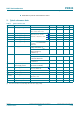
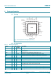
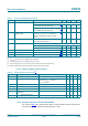
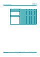
Table Of Contents
- 1. General description
- 2. Features and benefits
- 3. Quick reference data
- 4. Ordering information
- 5. Block diagram
- 6. Pinning information
- 7. Limiting values
- 8. Recommended operating conditions
- 9. Thermal characteristics
- 10. Characteristics
- 10.1 Power management characteristics
- 10.2 Antenna presence self test thresholds
- 10.3 Typical 27.12 MHz Crystal requirements
- 10.4 Pin characteristics for 27.12 MHz XTAL Oscillator (OSCIN, OSCOUT)
- 10.5 RSTPD_N input pin characteristics
- 10.6 Input pin characteristics for I0, I1 and TESTEN
- 10.7 RSTOUT_N output pin characteristics
- 10.8 Input/output characteristics for pin P70_IRQ
- 10.9 Input/output pin characteristics for P30 / UART_RX, P31 / UART_TX, P32_INT0, P33_INT1
- 10.10 Input/output pin characteristics for P35
- 10.11 Input/output pin characteristics for DP and DM
- 10.12 Input pin characteristics for SCL
- 10.13 Input/output pin characteristics for SDA
- 10.14 Output pin characteristics for DELATT
- 10.15 Input pin characteristics for SIGIN
- 10.16 Output pin characteristics for SIGOUT
- 10.17 Input/output pin characteristics for P34
- 10.18 Output pin characteristics for LOADMOD
- 10.19 Input pin characteristics for RX
- 10.20 Output pin characteristics for AUX1/AUX2
- 10.21 Output pin characteristics for TX1/TX2
- 10.22 System reset timing
- 10.23 Timing for the I2C-bus interface
- 10.24 Temperature sensor
- 11. Application information
- 12. Abbreviations
- 13. Revision history
- 14. Legal information
- 15. Contact information
- 16. Tables
- 17. Figures
- 18. Contents

PR533_SDS All information provided in this document is subject to legal disclaimers. © NXP Semiconductors N.V. 2014. All rights reserved.
Product short data sheet
COMPANY PUBLIC
Rev. 3.6 — 27 October 2014
206436 6 of 36
NXP Semiconductors
PR533
USB NFC integrated reader solution
OSCIN 15 I AVDD crystal oscillator input: input to the inverting amplifier of the oscillator. This pin
is also the input for an externally generated clock (f
clk
= 27.12 MHz).
OSCOUT 16 O AVDD crystal oscillator output: output of the inverting amplifier of the oscillator.
I0 17 I DVDD interface mode lines: selects the used host interface; in test mode I0 is used
as test signals.
I1 18 I DVDD
TESTEN 19 I DVDD test enable pin:
when set to 1 enable the test mode.
when set to 0 reset the TCB and disable the access to the test mode.
P35 20 I/O DVDD general purpose I/O signal
P70_IRQ 21 I/O PVDD interrupt request: output to signal an interrupt event to the host (Port 7 bit 0)
RSTOUT_N 22 O PVDD output reset signal; when LOW it indicates that the circuit is in reset state.
DVSS 23 G digital ground
DM 24 I/O PVDD USB D data line in USB mode or TX in HSU mode; in test mode this signal
is used as input and output test signal
DP 25 I/O PVDD USB D+ data line in USB mode or RX in HSU mode; in test mode this signal
is used as input and output test signal.
PVDD 26 P I/O pad power supply
DELATT 27 O PVDD optional output for an external 1.5 k resistor connection on D+.
P30 28 I/O PVDD general purpose I/O signal. Can be configured to act either as RX line of the
second serial interface UART or general purpose I/O.
In test mode this signal is used as input and output test signal.
P31 29 I/O PVDD general purpose I/O signal. Can be configured to act either as TX line of the
second serial interface UART or general purpose I/O.
In test mode this signal is used as input and output test signal.
P32_INT0 30 I/O PVDD general purpose I/O signal. Can also be used as an interrupt source
In test mode this signal is used as input and output test signal.
P33_INT1 31 I/O PVDD general purpose I/O signal. Can be used to generate an HZ state on the out-
put of the selected interface for the Host communication and to enter into
power-down mode without resetting the internal state of PR533.
In test mode this signal is used as input and output test signal.
P50_SCL 32 I/O DVDD I
2
C-bus clock line - open-drain in output mode
SDA 33 I/O DVDD I
2
C-bus data line - open-drain in output mode
P34 34 I/O SVDD general purpose I/O signal or clock signal for the SAM
SIGOUT 35 O SVDD contactless communication interface output: delivers a serial data stream
according to NFCIP-1 and output signal for the SAM.
In test mode this signal is used as test signal output.
SIGIN 36 I SVDD contactless communication interface input: accepts a digital, serial data
stream according to NFCIP-1 and input signal from the SAM.
In test mode this signal is used as test signal input.
SVDD 37 P output power for SAM power supply. Switched on by Firmware with an over-
load detection. Used as a reference voltage for SAM communication.
Table 3. PR533 pin description
…continued
Symbol Pin Type Pad ref
voltage
Description