
User's Manual
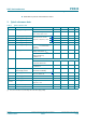
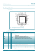
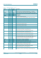
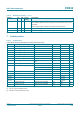
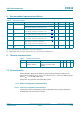
Table Of Contents
- 1. General description
- 2. Features and benefits
- 3. Quick reference data
- 4. Ordering information
- 5. Block diagram
- 6. Pinning information
- 7. Limiting values
- 8. Recommended operating conditions
- 9. Thermal characteristics
- 10. Characteristics
- 10.1 Power management characteristics
- 10.2 Antenna presence self test thresholds
- 10.3 Typical 27.12 MHz Crystal requirements
- 10.4 Pin characteristics for 27.12 MHz XTAL Oscillator (OSCIN, OSCOUT)
- 10.5 RSTPD_N input pin characteristics
- 10.6 Input pin characteristics for I0, I1 and TESTEN
- 10.7 RSTOUT_N output pin characteristics
- 10.8 Input/output characteristics for pin P70_IRQ
- 10.9 Input/output pin characteristics for P30 / UART_RX, P31 / UART_TX, P32_INT0, P33_INT1
- 10.10 Input/output pin characteristics for P35
- 10.11 Input/output pin characteristics for DP and DM
- 10.12 Input pin characteristics for SCL
- 10.13 Input/output pin characteristics for SDA
- 10.14 Output pin characteristics for DELATT
- 10.15 Input pin characteristics for SIGIN
- 10.16 Output pin characteristics for SIGOUT
- 10.17 Input/output pin characteristics for P34
- 10.18 Output pin characteristics for LOADMOD
- 10.19 Input pin characteristics for RX
- 10.20 Output pin characteristics for AUX1/AUX2
- 10.21 Output pin characteristics for TX1/TX2
- 10.22 System reset timing
- 10.23 Timing for the I2C-bus interface
- 10.24 Temperature sensor
- 11. Application information
- 12. Abbreviations
- 13. Revision history
- 14. Legal information
- 15. Contact information
- 16. Tables
- 17. Figures
- 18. Contents

PR533_SDS All information provided in this document is subject to legal disclaimers. © NXP Semiconductors N.V. 2014. All rights reserved.
Product short data sheet
COMPANY PUBLIC
Rev. 3.6 — 27 October 2014
206436 9 of 36
NXP Semiconductors
PR533
USB NFC integrated reader solution
[1] I
pd
is the total currents over all supplies.
[2] I
DD(PVDD)
depends on the overall load at the digital pins.
[3] I
DD(SVDD)
depends on the overall load on V
DD(SVDD)
pad.
[4] I
DD(TVDD)
depends on V
DD(TVDD)
and the external circuitry connected to TX1 and TX2.
[5] During operation with a typical circuitry the overall current is below 100 mA.
10.1.2 Voltage regulator characteristics
[1] The internal regulator is only enabled when the USB interface is selected by I0 and I1.
10.2 Antenna presence self test thresholds
The values in Table 9 are guaranteed by design. Only functional is done in production for
cases andet_ithl[1:0] = 10b and for andet_ithh[2:0] = 011b.
Table 7. Current consumption characteristics
Symbol Parameter Conditions Min Typ Max Unit
I
pd
power-down current V
DDA
= V
DDD
= V
DD(TVDD)
= V
DD(PVDD)
= 3 V; not powered from USB
hard power-down current; not powered
from USB; RF level detector off
[1]
-1.310A
soft power-down current; not powered
from USB; RF level detector on
[1]
-930A
I
CCSL
suspended low-power device
supply current
V
BUS
=5V; V
DDA
= V
DDD
= V
DD(TVDD)
=
V
DD(PVDD)
=3V; V
DDS
= 0 V; RF level
detector on (without resistor on pin DP
(D+))
[1]
- 120 250 A
I
DDD
digital supply current V
DDA
= V
DDD
= V
DD(TVDD)
= V
DD(PVDD)
= 3 V; RF level detector on
-12- mA
I
DDA
analog supply current V
DDA
= V
DDD
= V
DD(TVDD)
= V
DD(PVDD)
=3V
RF level detector on - 3 6 mA
RF level detector off - 1.5 5 mA
I
DD(PVDD)
PVDD supply current
[2]
--30mA
I
DD(SVDD)
SVDD supply current sam_switch_en set to 1
[3]
--30mA
I
DD(TVDD)
TVDD supply current continuous wave; V
DD(TVDD)
=3V
[4][5]
- 60 100 mA
Table 8. Voltage regulator characteristics
[1]
Symbol Parameter Conditions Min Typ Max Unit
V
BUS
bus supply voltage USB mode; V
SS
= 0 V 4.02 5 5.25 V
V
DDD
digital supply voltage after inrush current limitation (USB
mode); from I
VDDD
= 0 mA to
I
VDDD
=150mA
2.95 3.3 3.6 V
I
BUS
bus supply current USB mode; measure on V
BUS
--150mA
I
inrush(lim)
inrush current limit at power-up (curlimofff = 0) - - 100 mA
V
th(rst)reg
regulator reset threshold voltage regulator reset 1.90 2.15 2.40 V
V
th(rst)reg(hys)
regulator reset threshold voltage
hysteresis
35 60 85 mV
V
DDD
decoupling capacitor 8 10 - F